


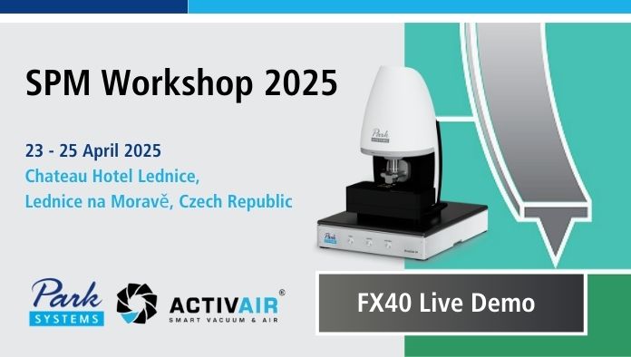
Join us and our distributor ActivAir for the SPM Workshop in Lednice, Czech Republic, hosted by the Department of Primary Nanometrology and Technical Length at the Czech Metrology Institute! This is a prime opportunity for professionals in the SPM field across Central Europe to come together, exchange groundbreaking research ideas, and explore topics like Novel SPM modes, UHV STM and AFM, and advancements in instrumentation. The event features engaging sessions with invited lectures and participant presentations.
@
Date: 23-25 Apri, 2025
Location: Chateau Hotel Lednice, Czech Republic
Don't miss the chance to see our FX40 AFM in action and hear Dr. Martin Rejhorn from Charles University talk about "Exploring ABC-stacked graphene domains in untwisted epitaxial graphene." Experience innovation and collaboration at this exciting workshop!
Abstract:
In graphene, emergent properties such as superconductivity to ferroelectricity have been observed in ABC-stacked domains, typically obtained by exfoliation followed by expert mechanical twisting and alignment with the desired orientation, a process very challenging and nonscalable. Here, we demonstrate that graphene in the ABC stacking domain can be obtained using a scalable growth technique, namely, the thermal decomposition of silicon carbide. Using conductive atomic force microscopy (Fig. 1a), we identified distinct conductivity patterns in untwisted three-layered epitaxial graphene on silicon carbide.
These patterns revealed the presence of ABA and ABC domains, matching the conductivity differences observed in twisted exfoliated graphene and those predicted by density functional theory. The size and geometry of the stacking domains depend on the interplay between strain, solitons crossing, and shape of the three-layer regions. Interestingly, we demonstrate the growth of three-layer regions in which the ABA/ABC stacking domains self-organize in stable stripes of a few tens of nanometers (Fig. 1b). This study demonstrates the potential of the thermal decomposition method for producing ABA/ABC domains, paving the way for future applications in electronic and optoelectronic devices.
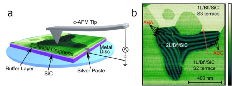
Figure 1: a) Setup of conductive AFM experiment. b) c-AFM image of an epitaxial graphene film with visible stripes in conductivity on a three layeref epitaxial graphene.