


-
Bio Ferroelectric Ucl LiquidCrystal Tungsten_disulfide Copolymer Celebration GaP INSPParis Galfenol ItoGlass Chrome Blood Polyvinylidene_fluoride heterojunctions University_of_Regensburg BlockCopolymer SRAM ForceVolumeImage AtomicSteps Lift Silver Sulfur PinpointNanomechanicalMode graphene_hybrid Ceramics Hexacontane Temasek_Lab LMF Semiconductor MESA structure SKKU PetruPoni_Institute lithography LaAlO3
Report image
If you found this image unacceptable, please let us know. We will review your report and take action if we determine this image is really unacceptable.
Monolayer Graphene on PDMS Surface
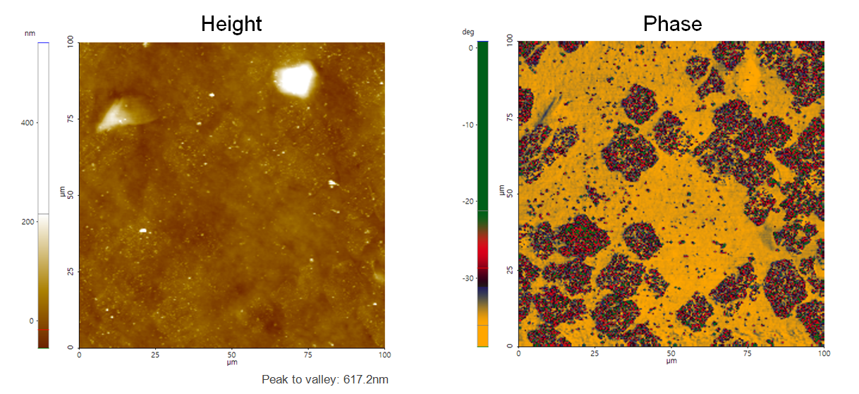
Monolayer Graphene grown on Cu foil using CVD process is transferred on to PDMS substrate.
Scanning Conditions
- System: NX20
- Scan Mode: Tapping
- Cantilever: Access-NC (k=113N/m, f=330kHz)
- Scan Size: 100μm×100μm
- Scan Rate: 0.6Hz
- Pixel Size: 256 × 256
- Scan Mode: Tapping
- Cantilever: Access-NC (k=113N/m, f=330kHz)
- Scan Size: 100μm×100μm
- Scan Rate: 0.6Hz
- Pixel Size: 256 × 256