


-
Fiber LDPE C_AFM TempControl STO NUS FM-KPFM LaAlO3 tip_bias_mode Ferrite Pyroelectric CP-AFM PatternedSapphireSubstrat Fendb Inorganic_Compound mechanical property PvdfBead SAM StyreneBeads Bmp Topography PolycrystallineFerroelectricBCZT GaN Stiffness LeakageCurrent Conductivity University_of_Regensburg F14H20 Polydimethylsiloxane Fujian Conduct Dimethicone Titanate Reduction PDMS
Report image
If you found this image unacceptable, please let us know. We will review your report and take action if we determine this image is really unacceptable.
Atomic steps on GaP(Gallium Phosphide) layer on Si
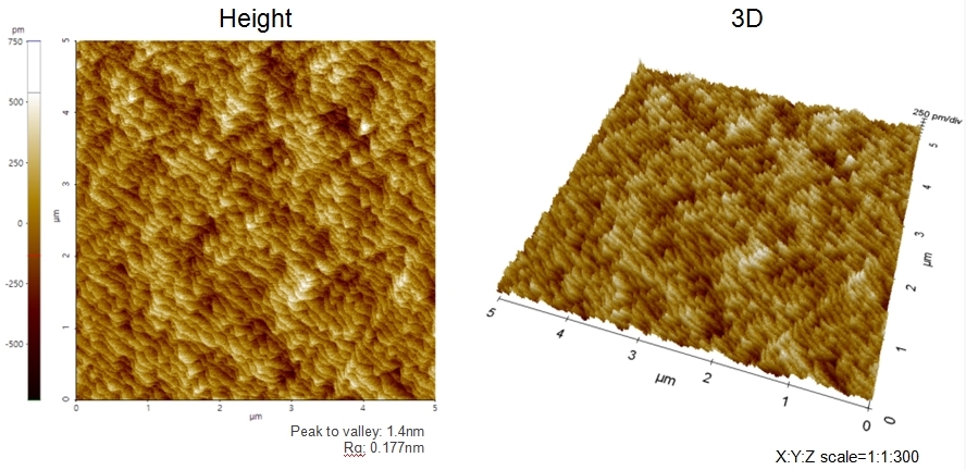
Scanning Conditions
- System: NX20
- Scan Mode: Non-contact
- Cantilever: PPP-NCHR (k=42N/m, f=300kHz)
- Scan Size: 5μm×5μm
- Scan Rate: 1Hz
- Pixel: 512×512