


-
LowDensityPolyethylene PyroelectricDetector Cell Magnetic ConductingPolymer Hole Piezo SiliconCrystal Ram VerticalPFM Chloroform CaMnO3 Chemical Vapor Deposition high_resolution polymeric_arrays Adhesion OpticalModulator YszSubstrate ContactModeDots CrossSection ScanningTunnelingMicroscopy DLaTGS Scanning_Thermal_Microscopy Ca10(PO4)6(OH)2 H-BN Global_Comm BTO PvdfBead cannabidiol Polystyrene Techcomp CeNSE_IISc amplitude_modulation OrganicSemiconductor Display
Report image
If you found this image unacceptable, please let us know. We will review your report and take action if we determine this image is really unacceptable.
AlN/GaN/AlN Hetero Structure
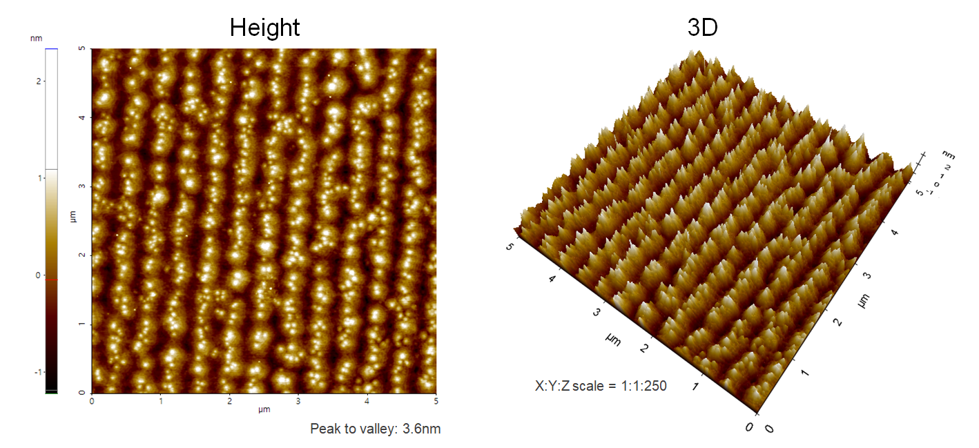
AlN/GaN/AlN hetero structure grown on SiC substrate by Molecular Beam Epitaxy (MBE) system.
Scanning Conditions
- System: NX20
- Scan Mode: Non-contact
- Cantilever: AC160TS (k=26N/m, f=300kHz)
- Scan Size: 5μm×5μm
- Scan Rate: 0.5Hz
- Pixel Size: 512 × 512
- Scan Mode: Non-contact
- Cantilever: AC160TS (k=26N/m, f=300kHz)
- Scan Size: 5μm×5μm
- Scan Rate: 0.5Hz
- Pixel Size: 512 × 512