


-
Sic SrTiO3 InLiquid Stiffness SiWafer FM-KPFM Tape MonoLayer GaP Pore BariumTitanate LithiumNiobate AdhesionEnergy lithography non_contact Sulfur alkanes Electrical&Electronics SoftSample semifluorinated alkane cooling NiFe ElectroChemical Calcium Optoelectonics Perovskite Praseodymium OpticalElement pulsed_laser_deposition Edwin OpticalWaveguides HighAcpectRatio HexagonalBoronNitride Fluoride Monisha
Report image
If you found this image unacceptable, please let us know. We will review your report and take action if we determine this image is really unacceptable.
Monolayer Graphene on PDMS Surface
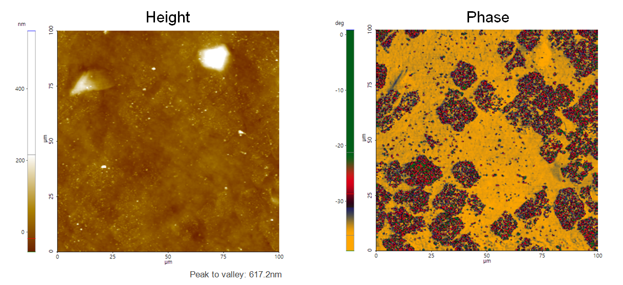
Monolayer Graphene grown on Cu foil using CVD process is transferred on to PDMS substrate.
Scanning Conditions
- System: NX20
- Scan Mode: Tapping
- Cantilever: Access-NC (k=113N/m, f=330kHz)
- Scan Size: 100μm×100μm
- Scan Rate: 0.6Hz
- Pixel Size: 256 × 256
- Scan Mode: Tapping
- Cantilever: Access-NC (k=113N/m, f=330kHz)
- Scan Size: 100μm×100μm
- Scan Rate: 0.6Hz
- Pixel Size: 256 × 256