


-
StainlessSteel silicon_carbide Conductive AFM exfoliate molecular_beam HfO2 semifluorinated_alkanes NCM\ StrontiuTitanate SPMLabs WPlug ElectroDeposition Foil SiliconeOxide norganic Thermal Multiferroic_materials Austenite Zagreb AM_KPFM China Pores LateralPFM Logo Etch Imprint membrane ReflexLens LightEmission Graphene Phenanthrene Lift Polydimethylsiloxane Step IndiumTinOxide
Report image
If you found this image unacceptable, please let us know. We will review your report and take action if we determine this image is really unacceptable.
PS/LPDE
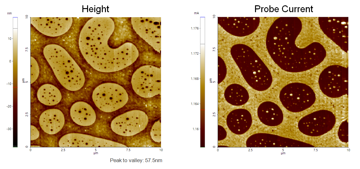
Spincast layer of PS/LDPE blend on Si. Signal change by thermal conductivity difference.
Scanning Conditions
- System: NX10
- Scan Mode: SThM
- Cantilever: NanoThermal Probe
- Scan Size: 10μm×10μm
- Scan Rate: 0.5Hz
- Pixel Size: 256 × 512
- Scan Mode: SThM
- Cantilever: NanoThermal Probe
- Scan Size: 10μm×10μm
- Scan Rate: 0.5Hz
- Pixel Size: 256 × 512