


-
UnivOfMaryland Organic Layer GaP AtomicSteps Nickel PolymerPatterns LateralForceMicroscopy Conduct Solution LDPE MBE HexagonalBoronNitride SolarCell Austenite SelfAssembly ImideMonomer Electronics Piranha mono_layer Galfenol MechanicalProperty StrontiuTitanate AM_SKPM fluoroaalkane dielectric_trench OpticalWaveguides SrTiO3 Chungnam_National_University atomic_steps AAO Electical&Electronics #EC lithography Mobile
Report image
If you found this image unacceptable, please let us know. We will review your report and take action if we determine this image is really unacceptable.
PMN-PT single crystal
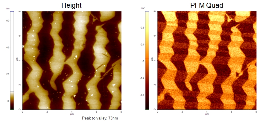
Scanning Conditions
- System: NX10
- Scan Mode: PFM
- Cantilever: NSC36A Ti-Pt (k=1N/m, f=90kHz)
- Scan Size: 8μm×8μm
- Scan Rate: 0.5Hz
- Pixel: 512×256