


-
Organic oxide_layer Beads Conducting thermoplastic_elastomers PolyvinylideneFluoride non_contact P3HT HexagonalBoronNitride AM_SKPM EvatecAG Implant Magnetostrictive CancerCell GranadaUniv ScanningTunnelingMicroscopy LDPE Bio MonoLayer ElectroDeposition CuParticle Temasek_Lab optoelectronics Melt Platinum Calcite Pinpoint PFM PhaseTransition hard_disk SetpointMode Stiffness HighAspect Mechanical&nanotechnology Memory LiNbO3
Report image
If you found this image unacceptable, please let us know. We will review your report and take action if we determine this image is really unacceptable.
Trench Etch Profile on Si Wafer
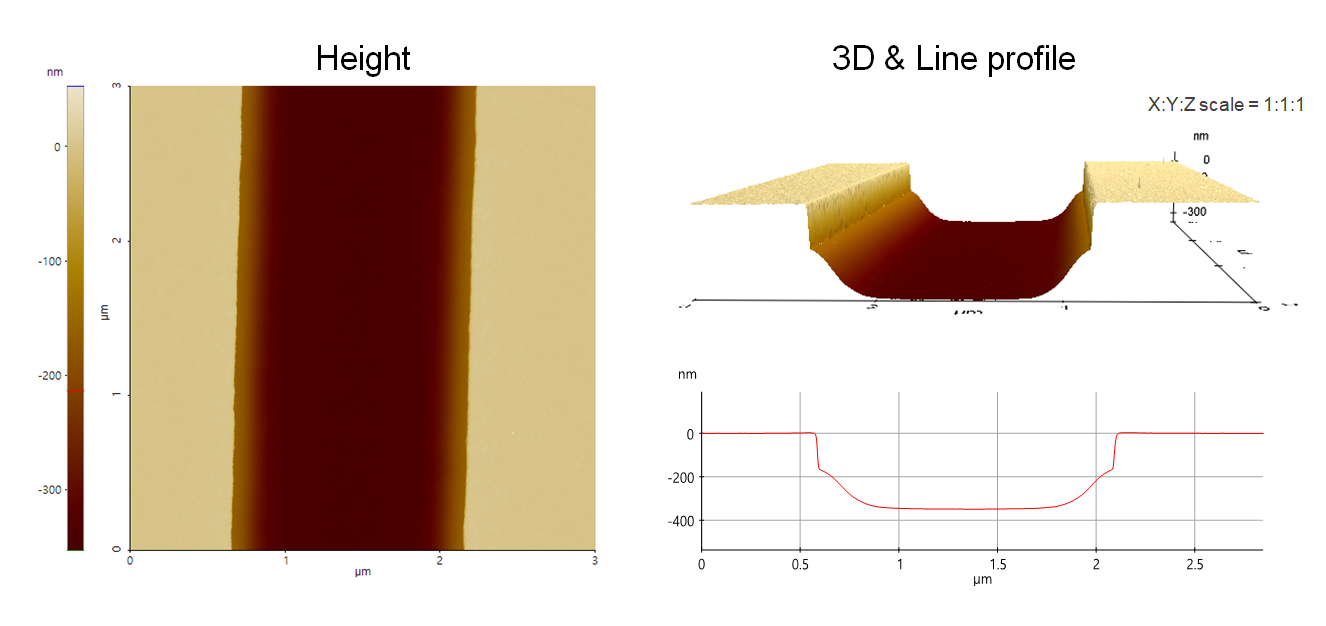
Top dielectric trench etch profile on Si wafer having tapered slope at the trench sidewall.
Scanning Conditions
- System: NX20
- Scan Mode: Non-contact
- Cantilever: AC160TS (k=26N/m, f=300kHz)
- Scan Size: 3μm×3μm
- Scan Rate: 0.21Hz
- Pixel: 1024 × 256
- Scan Mode: Non-contact
- Cantilever: AC160TS (k=26N/m, f=300kHz)
- Scan Size: 3μm×3μm
- Scan Rate: 0.21Hz
- Pixel: 1024 × 256