ISE meets AFM: A deeper understanding of complex surface system
maging spectroscopic ellipsometry (ISE) is an instrument that combines the measurement capabilities of an ellipsometer with the imaging capabilities of an optical microscope. ISE is capable of measuring ellipsometric parameters delta and psi at every single pixel within the microscope’s field of view. Spatial resolution of the ISE is defined by the instrument imaging optics and the detector pixel size.
Thus, ISE can resolve microscopic structure of the sample under study with the spatial resolution as small as a micron. In terms of vertical resolution, single and multi-layer structured samples with individual layer thicknesses ranging from few angstroms to few ten microns are within the measurement capability of the ISE. In addition, optical constants such as refractive index, extinction coefficient, and dielectric functions can be simultaneously determined from the ISE measurement.
Atomic force microscopy (AFM) is undoubtedly a powerful nanoscopic measurement tool. In AFM measurement, a sharp tip senses the sample surface and gives information on surface topography as well as various physical and chemical properties. The spatial resolution of AFM is limited by the curvature radius of the tip being used, which is typically larger than a few nanometers. Since the AFM tip is in contact with sample surface, a tip/sample bias can be applied to probe nanoscopic electrical properties of the sample simultaneously with surface topography. AFM measurement can also be conducted in controlled environments such as controlled temperature and humidity, various gas atmospheres or aqueous solutions, and in vacuum. This allows studying of material properties in practical applications.
Amid high resolution, the AFM is mainly used to study the top surface of a sample. For applications that require characterization of sub-surface or fully cover layer, usability of AFM is limited unless the top layer is removed, or the sample is cross-sectioned since AFM measures thickness via a step edge. ISE, on the other hand, allows non-invasive and non-destructive measurement of a complex surface system or buried layers. In this regard, combining both ISE and AFM can be advantageous in non-destructively study of surface topography and optical properties [1,2]. In addition, this combination allows correlative study among optical properties, surface topography, and various physical properties of the sample, facilitating a deeper understanding of the sample’s characteristics.
Combined ISE and AFM studies of vdW heterostructure
This application note presents an example of the synergistic combination of ISE and AFM for characterization of 2-dimensional (2D) van der Waals (vdW) heterostructures. As a sample, twisted bilayer graphene (TBG) on hexagonal boron nitride (hBN) was prepared and characterized. The ISE was used to determine layer thickness and optical properties while the AFM was used to study Moiré superlattice formed by lattice mismatch of the layers.
A typical dry transfer technique was used to fabricate the TBG on hBN heterostructure sample. The mechanically exfoliated flakes were picked up and stacked sequentially using a polycarbonate (PC) film. First, a stack consisting of hBN/Graphite/TBG was prepared. Then, the stack was transferred to a gold-coated polydimethylsiloxane substrate. After that, the PC film was removed using N-methyl-2-pyrrolidone (NMP). Finally, the stack was stamped onto an SiO2/Si substrate with a pre-patterned electrode. A full experimental detail is described elsewhere [3]. Fig. 1(a) shows an optical image of the fabricated sample. Positions of the single layers of graphene (SLG) are marked with dashed orange lines. The overlapped area (TBG, blue shaded) is the region of interest (ROI) for both ISE and AFM measurements.
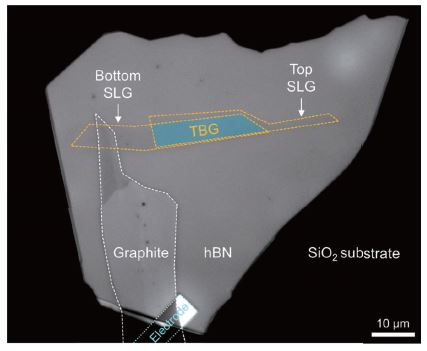
Fig. 1. (a) Optical image of the prepared sample. The graphene layers are marked with dashed orange lines.
The graphene flake on the left side is the bottom layer. The bottom graphene is connected to the pre-patterned electrode (cyan dotted line) via the graphite flake (white dashed line).
It should be noted that the sample preparation procedure described above results in a clean surface of TBG, which is beneficial for properties characterization. However, the backside of the hBN flake is prone to adsorbed water or hydrocarbon (HC) contamination after NMP washing. When the stack is transferred to the SiO2/Si substrate, the vdW force squeezes out and traps contaminants into small pockets (bubbles) at the hBN/SiO2 interface. Several studies have revealed that the bubbles act as local optical cavities and strain-induced local emitters, facilitating potential applications in optoelectronics and photonics [4,5]. It has also been found that the bubble improves electron transfer in 2D material-based memory devices [6]. Within the scope of this application note, the application of ISE in studying the effect of bubble formation on the optical properties of vdW heterostructure will also be introduced. Details will be given in the next section.
ISE measurement
Spectroscopic ellipsometry measurements were conducted using an imaging ellipsometer (Accurion EP4, Park Systems) equipped with a 20× objective and a CMOS detector. This configuration of optical components results in a spatial resolution down to 1 μm. A rotating compensator ellipsometry method was used to measure delta (Δ) and psi (Ψ) as a function of wavelength (λ). Polarizer and analyzer angles were fixed at 45°. Angle of incidence was set at 60°. The wavelength ranged from 360 to 800 nm at 5 nm intervals. The measurement was carried out under ambient conditions.
Example of Δ map result at 400 nm is shown in Fig. 2(a). As can be seen, various spots with different Δ contrast (spots with red color) were observed on the hBN flake, due to the presence of the bubbles. Those micron-sized bubble areas are not visible by optical microscopy (Fig. 1). Notably, there was also a bubble in the middle of the TBG area. The thicknesses of SiO2, hBN, TBG, and HC layers were determined from individual model fits to ROIs 1, 2, 3, and 4, respectively, as denoted in Fig. 2(a). The bubble at ROI 4 is assumed to be hydrocarbon in this work. To avoid data correlation between various fit parameters, the thickness of previously determined layer is used as a fixed parameter when fitting the later ROI. In more detail, the SiO2/Si model was applied to ROI 1 to determine the thickness of SiO2 layer. Next, SiO2 thickness is used as a fixed parameter when applying the hBN/SiO2/Si model to ROI 2 to calculate the thickness of hBN layer. The thicknesses of SiO2 and hBN are then used as fixed parameterswhen building the optical models for ROI 3 (TBG/hBN/SiO2/Si) and ROI 4 (TBG/hBN/HC/SiO2/Si). To model the TBG layer, an additional Gaussian term was added to account for the optical resonance resulting from the twist angle between two graphene layers [7]. The HC layer is modelled with Cauchy’s dispersion. The dispersions of other layers are either defined or taken from literature.
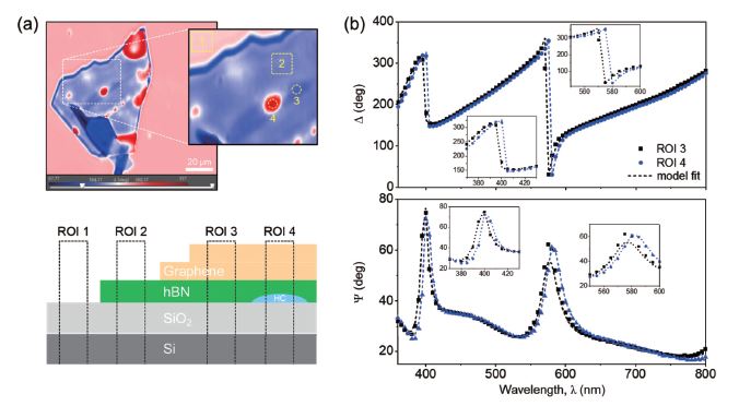
Fig. 2. (a) Δ map result at 400 nm and ROIs used for ellipsometry data analysis, and (b) Δ and Ψ spectra obtained on ROIs 3 and 4. In (b), the black and blue dots represent the experimental Δ and Ψ values while the black and blue dashed line represent the model fits to ROIs 3 and 4, respectively.
The insets display zoomed views of the data at two significant oscillation peaks.
Plots of experimental and model fits to Δ and Ψ values obtained from ROIs 3 and 4 are shown in Fig. 2(b). In general, the Δ and Ψ curves obtained from both ROIs show similar oscillations. However, an offset towards longer wavelength can be clearly observed for both Δ and Ψ data in the presence of the bubble. The thickness calculation results are summarized in Table 1. The thickness of the bilayer graphene layer was determined to be 0.699 ± 0.002 nm, which is in good agreement with previously reported result [8]. The determined thickness of the hydrocarbon layer was 7.343 ± 0.015 nm.
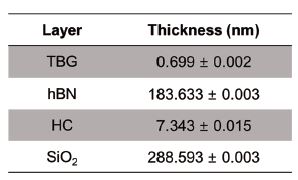
Table 1. Summary of the layer thickness determined from ISE data. Error represents one standard deviation of the fit.
As aforementioned, the presence of the bubble can change the optical properties of the heterostructure sample. To investigate the effect of bubble formation on the optical properties of the sample, optical constants such as refractive index (n), extinction coefficient (k), and absorbance (A) of the TBG layer as is (ROI 3) and in the presence of the bubble (ROI 4) are calculated, as shown in Fig. 3. The values of n, k, and A are determined simultaneously with the thickness from optical model fits to ROIs 3 and 4. The absorbance is calculated using equation A=4πnkt/λ, where t is the thickness of TBG layer [9]. It was found that the refractive index generally decreases while the extinction coefficient increases in the presence of the bubble. As a result, the calculated A values from ROIs 3 and 4 agree within the wavelength range from 360 to 550 nm, while a significant absorbance difference is observed at wavelengths from 550 to 800 nm, due to the presence of the bubble. Lower absorbance % at ROI 4 suggests a reduced absorption in the photonics devices at given wavelength in the range from 550 to 800 nm.
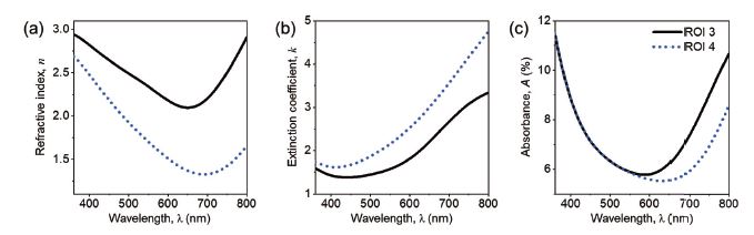
Fig. 3. (a) Refractive index, (b) extinction coefficient, and (c) absorbance vs. wavelength of the TBG layer as is (ROI 3) and in the presence of the bubble (ROI 4).
AFM measurement
AFM measurement was conducted using an automated AFM (FX200, Park Systems) equipped with a current amplifier. Park's FX200 is an AFM system launched targeting small (a few centimeters) to large samples of 200 mm in size, but due to its high performance based on extremely low noise level, minimal thermal drift, and exceptional stability, it shows all features clearly even in scan sizes of 100 nm2 or less. A metal-coated AFM tip was used to collect the data on the sample. To locate the regions of interest, tapping mode of AFM was used to minimize the damage to the tip and sample. Fig. 4 shows topography images obtained on the sample. The AFM images are overlaid on the optical image for better visualization of the sample structure. The thicknesses of hBN and graphene layers were also determined, as denoted in the figure. Layer thickness determined from the AFM data was found to be in good agreement with those determined from the ISE measurement. The deviation between thickness of HC layer determined by ISE and AFM may be associated with data averaging over the entire selected area when capturing Δ and Ψ data at ROI 4. It should be noted that to calculate the thickness using AFM, each individual flake should be exposed since AFM measures thickness via a step edge. In this sense, AFM measurement is more suitable for samples that have partially cover layers. For a fully covered surface, ISE measurement can provide an accurate result while preserving the sample integrity.
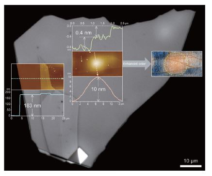
Fig. 4. Topography images and cross-sectioned line profiles obtained at different locations on the sample.
After locating ROIs 3 and 4, using the same AFM tip, the scan mode was switched to conductive AFM (C-AFM) to perform high magnification scans to visualize the Moiré superlattice of the sample. During C-AFM, a DC sample bias is applied to the electrode via the AFM sample holder. In this way, the current flows from the electrode to the graphite flake, then to the bottom graphene flake, and finally
to the top graphene flake. The AFM tip is then used to map the current distribution across the surface of the TBG layer. The current images obtained at ROIs 3 and 4 are presented in Fig. 5. Moiré patterns with different periods were observed at the two ROIs, as denoted in the cross-sectional line profiles in Fig. 5. The difference in periodicity is associated with different stacking registries, which is typically observed in the literature [10–12]. The current signal ranges from 1.5 to 2.2 nA (peak-to-valley of 0.7 nA) for ROI 4 and 15 to 125 pA (peak-to-valley of 0.11 nA) for ROIs 3, from the line profiles in Fig. 5. The difference in applied contact force during the measurements, which were approximately 10 nN for ROI 4 and 5 nN for ROI 3, may be the reason for this observation. Considering that the contrast mechanism for C-AFM measurement is the contact resistance at local tip-graphene junction, a higher contact force yields a larger contact area, allowing more current to flow through.
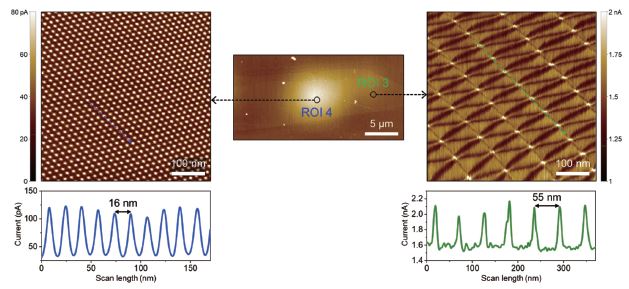
Fig. 5. Current images and cross-sectioned line profiles obtained at different locations on the TBG layer. The scan rate was set to 10 Hz.
A DC bias of 10 mV was applied to the sample during measurement. Contact forces were 5 nN for ROI 3 and 10 nN for ROI 4.
It is worth noting that the tip used for C-AFM measurement has a nominal radius of curvature of 30 nm. In fact, metal-coated tips used for electrical measurements typically have radii of larger than few tens of nm. However, as experimentally observed in Fig. 5, the tip can still resolve a high spatial resolution better than a few nanometers. A plausible explanation for this outcome is that the main quantification
to define spatial resolution is the tip-sample contact radius (which is proportional to contact force). In general, a larger contact force helps to improve the surface tracking, however, decreases the spatial resolution of measurement due to large contact radius. Besides, for small scan size scan, a high scan rate is preferred to reduce scanner drift and low frequency acoustic noise. To optimize the image quality with a given tip, it is suggested that the contact force should be minimized, and the scan rate should be maximized while still maintaining good surface tracking.
In addition to C-AFM, various electrical modes of the AFM have been utilized for visualization of the Moiré superlattice such as piezoelectric force microscopy (PFM) and scanning microwave impedance microscopy (sMIM) [10–12]. Moiré pattern measurements based on PFM typically require resonance enhancement (CR-PFM) or dual frequency resonance tracking (DFRT-PFM) mode, while specialized AFM
tip and hardware are needed to perform an sMIM imaging. C-AFM on the other hand has the advantage of simplicity of setup and operation and is readily available in almost all conventional AFMs.
Summary and prospects
The use of both methods, ISE and AFM, increases confidence in the correctness of the trapped HC bubble assumptions and is a good example on how imaging spectroscopic ellipsometry and atomic force microscopy can be combined to attain a deeper understanding of complex surface systems. In particular, the ISE was used to study the optical properties and effect of a bubble on optical properties while the AFM is used to characterize the Moiré superlattice of twisted bilayer graphene on hBN vdW heterostructure sample. The results obtained from both methods offer a thorough understanding of properties of the heterostructure sample, from microscopic view on how the sample interacts with incident light to nanoscopic view on morphology and electrical characteristics. We believe that this synergic combination can provide new characterization tools to the emerging field of optoelectronics and photonics.
Acknowledgements
The author thanks Prof. Tomoki Machida and their group members, especially Yuta Seo and Jimpei Kawase at Institute of Industrial Science, The University of Tokyo for helping with sample preparation and fruitful discussions on the measurement results.
References
[1] E.L.H. Thomas, S. Mandal, Ashek-I-Ahmed, J.E. Macdonald, T.G. Dane, J. Rawle, C.-L. Cheng, O.A. Williams,
Spectroscopic Ellipsometry of Nanocrystalline Diamond Film Growth, ACS Omega. 2 (2017) 6715–6727.
[2] P. Kaspar, D. Sobola, R. Dallaev, S. Ramazanov, A. Nebojsa, S. Rezaee, L. Grmela, Characterization of Fe2O3
thin film on highly oriented pyrolytic graphite by AFM, Ellipsometry and XPS, Appl. Surf. Sci. 493 (2019) 673–678.
[3] H. Kim, Y. Choi, É. Lantagne-Hurtubise, C. Lewandowski, A. Thomson, L. Kong, H. Zhou, E. Baum, Y. Zhang, L. Holleis, K. Watanabe, T.
Taniguchi, A.F. Young, J. Alicea, S. Nadj-Perge, Imaging inter-valley coherent order in magic-angle twisted trilayer graphene, Nature. 623
(2023) 942–948.
[4] Z. Jia, J. Dong, L. Liu, A. Nie, J. Xiang, B. Wang, F. Wen, C. Mu, Z. Zhao, B. Xu, Y. Gong, Y. Tian, Z. Liu, Photoluminescence and Raman
Spectra Oscillations Induced by Laser Interference in Annealing-Created Monolayer WS2 Bubbles, Adv. Opt. Mater. 7 (2019) 1801373.
[5] A. V Tyurnina, D.A. Bandurin, E. Khestanova, V.G. Kravets, M. Koperski, F. Guinea, A.N. Grigorenko, A.K. Geim, I. V Grigorieva,
Strained Bubbles in van der Waals Heterostructures as Local Emitters of Photoluminescence with Adjustable Wavelength, ACS Photonics. 6
(2019) 516–524.
[6] O.H. Gwon, S.G. Jang, J.Y. Kim, H.S. Kim, Y.-J. Yu, Electron Tunneling Enhancement in MoS2/Hexagonal Boron Nitride/Multilayer
Graphene Heterostructures by Bubble Formation, Appl. Sci. Converg. Technol. 31 (2022) 110–112.
[7] T. Potočnik, O. Burton, M. Reutzel, D. Schmitt, J.P. Bange, S. Mathias, F.R. Geisenhof, R.T. Weitz, L. Xin, H.J. Joyce, S. Hofmann, J.A.
Alexander-Webber, Fast Twist Angle Mapping of Bilayer Graphene Using Spectroscopic Ellipsometric Contrast Microscopy, Nano Lett. 23
(2023) 5506–5513.
[8] A.M. Affoune, B.L. V Prasad, H. Sato, T. Enoki, Y. Kaburagi, Y. Hishiyama, Experimental evidence
of a single nano-graphene, Chem. Phys. Lett. 348 (2001) 17–20.
[9] A.N. Toksumakov, G.A. Ermolaev, M.K. Tatmyshevskiy, Y.A. Klishin, A.S. Slavich, I. V Begichev, D. Stosic, D.I. Yakubovsky, D.G.
Kvashnin, A.A. Vyshnevyy, A. V Arsenin, V.S. Volkov, D.A. Ghazaryan, Anomalous optical response of graphene on hexagonal boron nitride
substrates, Commun. Phys. 6 (2023) 13.
[10] L.J. McGilly, A. Kerelsky, N.R. Finney, K. Shapovalov, E.-M. Shih, A. Ghiotto, Y. Zeng, S.L. Moore, W. Wu, Y. Bai, K. Watanabe, T.
Taniguchi, M. Stengel, L. Zhou, J. Hone, X. Zhu, D.N. Basov, C. Dean, C.E. Dreyer, A.N. Pasupathy, Visualization of moiré superlattices, Nat.
Nanotechnol. 15 (2020) 580–584.
[11] A.C. Gadelha, D.A.A. Ohlberg, F.C. Santana, G.S.N. Eliel, J.S. Lemos, V. Ornelas, D. Miranda, R.B. Nadas, K. Watanabe, T. Taniguchi,
C. Rabelo, P.P. de M. Venezuela, G. Medeiros-Ribeiro, A. Jorio, L.G. Cançado, L.C. Campos, Twisted Bilayer Graphene: A Versatile Fabrication
Method and the Detection of Variable Nanometric Strain Caused by Twist-Angle Disorder, ACS Appl. Nano Mater. 4 (2021)
1858–1866.
[12] X. Huang, L. Chen, S. Tang, C. Jiang, C. Chen, H. Wang, Z.-X. Shen, H. Wang, Y.-T. Cui, Imaging Dual-Moiré Lattices in Twisted
Bilayer Graphene Aligned on Hexagonal Boron Nitride Using Microwave Impedance Microscopy, Nano Lett. 21 (2021) 4292–4298.