Abstract
This study explores the electronic properties of low-angle twisted bilayer graphene (tBG) prepared on hexagonal boron nitride (hBN) flakes on a SiO2/Si substrate. Experimental investigations and simulation studies were conducted to understand the formation and characteristics of moiré patterns in tBG. Current maps revealed a smaller-scale moiré pattern with a symmetric hexagonal structure and an AA wavelength of approximately 6 nm, corresponding to a local twist angle of 2.35°. Conversely, a larger-scale moiré pattern displayed a subtly skewed honeycomb shape, with an average AA distance of 76 nm, resulting in a local twist angle of 0.19°. Simulation studies validated these experimental findings, confirming the accuracy of measured AA distances and domain sizes. Further characterization unveiled distinct conductive properties for different domains, with the AA inner domain exhibiting the highest conductivity among domains, reaching 3.47×10⁻⁵ S/cm under positive potential and 1.69×10⁻⁵ S/cm under negative potential. This comprehensive analysis provides valuable insights into the electronic behavior of low-angle tBG, paving the way for advancements in nanotechnology and quantum materials science.
Introduction
Manipulating the interlayer twist angle provides an effective method for adjusting the electronic characteristics of two-dimensional (2D) van der Waals (vdW) materials. Since the magic angle 1.1° of twisted bilayer graphene (tBG) is known for its remarkable electronic characteristics, various degrees of tBG have been studied to understand the underlying mechanisms .1,2 While previous studies examining the effects of interlayer twist on chemical reactivity have been reported, they have primarily focused on large twist angles (≥7°).3-5 The evolution of vertical conductivity in tBG with respect to twist angle at low-twist angles (< a few degrees), reveals several intriguing characteristics including vibration mode modulation, changes in electronic structure, and electron-photon coupling behavior. The competition among interlayer vdW interactions, atomic and electronic reconstruction becomes notable at small twist angles.6-8 The distance between AA domains, where the carbon atoms are directly aligned on top of each other, are highly relevant to the twist degree. Consequently, this leads to an enlargement or shrinkage of all other domains.9 Recently, C-AFM has been extensively utilized for studying tBG due to its high sensitivity to local conductivity variations and high spatial resolving power. This capability allows for the precise identification and characterization of stacking domains and their conductivity properties. In 2019, researchers investigated the transition in tBG from incommensurate to commensurate8 In 2020, a study demonstrated nonmonotonic vertical conductivity in tBG,10 while another explored symmetry breaking in 2022.11 Additionally, researchers presented two metastable reconstruction states in small-angle twisted monolayer–multilayer graphene in the same year.12 In this study, we employ C-AFM to characterize the moiré pattern of low-twist angle tBG and investigated its conductivity under both positive and negative potentials. The tBG sample investigated here is fabricated via graphene cutting using C-AFM,13 Our measurement reveals current maps of moiré patterns in two distinct scales within the sample. The local twist angles are accurately determined and uncovered deviations from intended values during fabrication. Moiré pattern simulations are employed to compare experimentally detected moiré wavelength and domain sizes, representing the methodology of understanding of tBG's complexity in electrical property.
Fabrication of tBG/hBN Heterostructure with Electrical Contacts
The twisted bilayer graphene sample was fabricated using the "tear and stack" technique in collaboration with Prof. Yu's group at George Mason University, VA, U.S. The fabrication process utilized a temperature-controlled heating stage (Instec), equipped with an optical microscope (Mitutoyo FS70) and a micromanipulator (MP-285, Sutter Instrument). Initially, a single large graphene sheet placed on a SiO2/Si substrate was divided into two pieces using C-AFM (Figure 1a, 1b). This step allowed for precise control over the rotation angle during the manual rotation process, minimizing fabrication errors in the twist angle between the two graphene layers (Figure 1c). In C-AFM, an AC bias was applied using one of the four built-in internal lock-in amplifiers (40 kHz, 10V for 20 min., relative humidity 40%, Park NX12 AFM). This resulted in a clean cut of the graphene at the junction of the conductive tip and the graphene surface, facilitated by the presence of high humidity in the ambient environment (Figure 1d). Su sequently, individual hexagonal boron nitride (hBN) flakes, ranging in thickness from 10 to 20 nm, were picked up from a SiO2/Si substrate using a thin poly(bisphenol-A carbonate) film attached to a polydimethylsiloxane stamp. These hBN flakes were aligned with half of a monolayer of graphene and torn along the edge of the hBN. The stage was then rotated to achieve the desired moiré twist angle (θm), and the picked-up graphene was carefully positioned over the remaining portion of the graphene to form the tBG/hBN heterostructure. To establish immediate electrical contact with the TBG, a thick graphite flake with thicknesses ranging from 10 to 100 nm was picked up to partially overlap with the graphene. Following the assembly of the heterostructure, the poly(bisphenol-A carbonate) film was delaminated from the polydimethylsiloxane stamp and transferred onto a fresh SiO2/Si chip(Figure 2a). Subsequently, tin/indium (Sn/In) contacts were created on the graphite contact using a micro-soldering method to facilitate electrical measurements. This fabrication process ensured precise alignment and integration of tBG/hBN heterostructures with reliable electrical contacts, enabling the investigation of their electronic properties and potential applications in nanoelectronics and quantum devices.
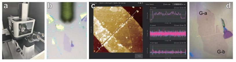
Figure 1. Procedure for cutting graphene for tBG sample preparation: (a) A picture of the Park NX12 AFM with a Faradaic cage equipped on an inverted optical microscope; (b) An optical micrograph showing a conductive cantilever (top-center) located near one graphene sheet on a Si substrate (bottom-center); (c) Screen view of SmartScanTM exhibiting anodic oxidation graphene cutting in progress, displaying the pre-acquired topography of the center part of a graphene flake, the typical cutting conditions were 40 kHz 10 V. under ambient relative humidity (~40%); (d) An optical micrograph showing the two graphene sheets clearly separated at the center after anodic oxidation cutting (into G-a and G-b).
Identification of Moiré Pattern Positions in the Fabricated tBG Sample.
The central region of the tBG area, outlined by a dashed square in Figure 2a, was analyzed using C-AFM, revealing two distinct moiré patterns. The surface of the tBG exhibited overall flatness and smoothness, devoid of small features. Notably, within this central region, one long graphene wrinkle was observed, accompanied by one lower height wrinkle in the perpendicular direction. As observed in the optical microscopic view (black square with dashed line in Figure 2a) as a circular purple area, a bubble was formed beneath the tBG,between the tBG/hBN layer and the polycarbonate film. This phenomenon often occurs during the tBG fabrication process. All measurements were carried out far away from the bubble. In the overlapping region of the 1st and 2nd graphene layers (Figure 2b), two distinct regions displaying different sizes of moiré patterns were identified in the current map of C-AFM. As described earlier, forming a solid electrical connection by placing graphite and a composite of indium and tin is of key importance to the successful C-AFM measurements. To verify proper electrical connectivity of the whole system, a conductive cantilever was scanned over the graphite at the left end of the scanned area (Figure 2b). It is worth noting that the moiré pattern observed in the current map was unique to the two regions (A and B) and was not observed in other areas of the fabricated graphene.
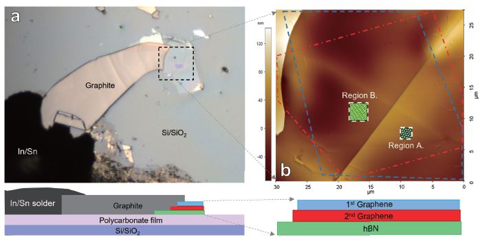
Figure 2. Fabricated tBG shown in optical micrograph (a) and AFM topography (b). In (a), the tBG was electrically connected with a piece of graphite soldered by a composite alloy of indium(In) and tin(Sn). The area marked with a dashed square in black was measured by contact mode AFM, revealing the tBG area in (b) with a distinctive linear wrinkle at the center spanning the entire tBG area. The first graphene layer is marked with a blue-thick dashed line in the AFM topography, while the second graphene layer is marked with a red-thick dashed line. Two different moiré patterns in conductive AFM measurements were observed in regions A and B, as indicated in the center of the AFM topography (b), including miniaturized corresponding moiré patterns in each region. As described at the bottom of (a) and (b), the tBG was formed on the surface of a single layer of hexagonal boron nitride placed on a layer of polycarbonate film (half a millimeter thick) attached to a Si/SiO2 substrate.
Conductive AFM Measurement
C-AFM enables simultaneous measurement of current and topography. Utilizing a Park NX20 AFM, C-AFM measurements were conducted on samples stored under ambient conditions for at least one week, with relative humidity maintained between 30-50%. A conductive tip, applying a constant force of 12 nN, scanned the graphene surface while current was recorded in raster scanning. The C-AFM setup employed a diamond tip (AD-2.8-SS, Adama Innovations) with a radius of 5.0 nm, heavily doped with boron and featuring a resistivity range of 0.003 - 0.005 Ω∙cm. During C-AFM measurement, separate electrical potentials were applied in trace and retrace scans, enhancing the accuracy of colocalized current maps in both negative and positive electric potentials. The picoampere current signal was recorded by an internal current amplifier of the AFM system.
C-AFM offers several advantages for the electrical property characterization of moiré patterns, such as those found in tBG.
- provides nanoscale spatial resolution, crucial for studying the fine details and variations in electronic behavior within moiré superlattices.
- measures local electrical properties directly at the nanoscale, essential for investigating heterogeneous electronic properties within moiré patterns.
- simultaneously acquires topographical, frictional, and electrical data, enabling correlation between physical structure and electrical characteristics.
- is sensitive to local defects and variations, allowing the study of phenomena like charge trapping and domain boundaries that affect electrical performance.
- provides quantitative measurements of electrical properties such as I-V characteristics, local conductivity, and resistance, aiding in the development of detailed electronic models.
- is compatible with various sample environments, enabling the study of moiré patterns under different conditions.
- is relatively non-destructive, making it suitable for characterizing sensitive materials like tBG without significant alteration.
Data Analysis and Moiré Patterns Simulation
Topography and current map data underwent analysis using SmartAnalysisTM software (Park Systems), and Gwyddion (Czech Metrology Institute), while Python scripts were employed to simulate moiré patterns with hexagonal unit cells at various rotation angles, along with corresponding overlap maps.
Results and Discussion
The tBG moiré patterns model and the associated theoretical framework provide critical insights into the unique electronic properties of twisted bilayer graphene. Understanding the formation of moiré patterns, the resulting electronic band structure, and the emergence of correlated electronic states are essential for advancing research and applications of tBG. The formation of moiré patterns in tBG occurs when two layers of graphene are stacked with a slight twist relative to each other. This twist causes interference between the periodic atomic lattices of the two layers, resulting in a moiré pattern. The periodicity of the resulting moiré superlattice depends on the twist angle between the layers. For low twist angles, the moiré pattern exhibits larger periodic structures, whereas high angles produce smaller periodic structures.
Moiré Pattern in Region A
In region A, moiré patterns exhibited a hexagonal shape with each corner decorated with circular units (AA (aligned stacking) in typical moiré pattern model) with an inter-AA distance of approximately 6 nm (Figure 3a and 3b). The hexagonal patterns exhibited identical positive and negative potentials, while the recorded current signals were opposite for positive and negative currents under applied potentials of ± 200 mV, with magnitudes in the picoampere range. The current map in Figure 3 represents a zoomed-in area, and the same pattern was observed across the entire area, which spanned several microns squared. Line profiles of each pattern (Figure 3c) illustrate the differing magnitudes of current values between positive and negative potentials, indicating that conductivity is higher under positive potential compared to negative.
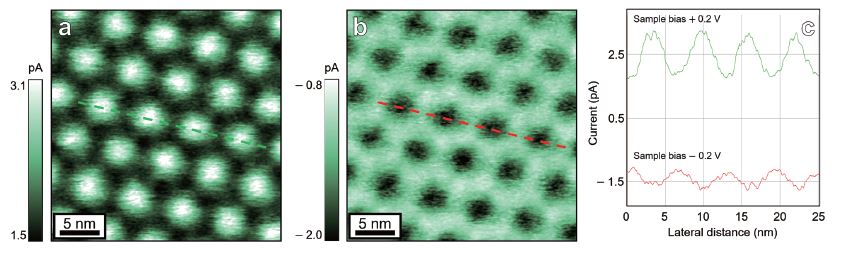
Figure 3. Current maps of the moiré pattern found in region A, measured by C-AFM, with +200 mV (a) and - 200 mV (b) applied to the tBG sample. Line profiles extracted from each dashed line are presented in plot (c), showing the recorded current range at +200 mV from 1.8 pA to 3.3 pA and at -200 mV from - 1.2 pA to - 1.8 pA. The corresponding C-AFM measurement conditions were as follows: cantilever AD-2.8-SS, scan rate 13 Hz (linerate), 1024 × 512 pixel, scan size 30 × 30 nm², dual bias imaging.
Moiré Pattern in Region B
In region B, moiré patterns were detected on a larger scale than in region A, displaying numerous triangular shapes and distinctly sized AA domains at each corner (light green in Figure 4a and dark green in Figure 4b). The average AA distance was about 75 nm. For both potentials, the moiré pattern consistently appeared in the same shapes with high repetition for the entire current map. Collecting six triangles forms a hexagonal unit cell of the moiré pattern. Within this hexagonal pattern, AB (Bernal stacking), BA (inverse Bernal stacking), and SP (saddle point) domains were clearly discernible in the current maps. The current values of the three domains between positive and negative potentials were inversely related. Line profiles of current extracted from both current maps are shown in Figure 4c. The positive current ranged from 1.5 pA to 6 pA, with the current at AA exhibiting values 2 to 3 times higher than in other domains. Similarly, the negative current ranged from -0.9 pA to -3.0 pA, with the current at AA also showing a higher magnitude than in other domains. It is noteworthy that no distinct features were observed in the topography and lateral (friction) force maps acquired concurrently. Further characterization revealed distinct classifications of conductivity for each domain, comprising AA inner and outer, AB, BA, and SP domains, under both positive and negative potentials. AA inner domain showed the highest conductivity in the range of 3.47×10⁻⁵ S/cm for positive potential and 1.69×10⁻⁵ S/cm for negative potential.
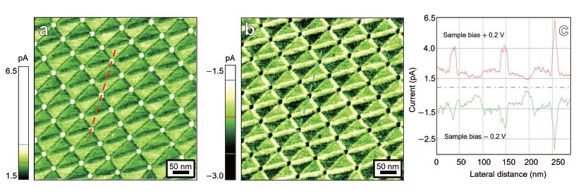
Figure 4. Current maps of the moiré pattern found in region B, measured by C-AFM, with +200 mV (a) and - 200 mV (b) applied to the tBG sample. Line profiles extracted from each dashed line are presented in plot (c), showing the recorded current range at +200 mV from 1.5 pA to 6.5 pA and at - 200 mV from - 0.9 pA to - 2.8 pA. The corresponding C-AFM measurement conditions were as follows: cantilever AD-2.8-SS, scan rate 6.5 Hz, 512 × 512 pixel, scan size 500 × 500 nm².
Individual Domain Maps and Statistical Analysis of the Moiré Patterns under Positive Potential (Region B)
The conductivity of individual domains within the moiré patterns was evaluated by carefully analyzing the current maps obtained under both positive and negative electric potentials (Figures 5 and 6). Each domain represents a distinct region within the moiré pattern, reflecting different stacking configurations or structural features of the material. These domains form under the influence of various interlayer forces, including van der Waals and electrostatic interactions. Additionally, mechanical deformations or strains within the tBG sample structure can also affect the stacking configuration and electronic properties. Here, the hexagonal unit cell appears compressed in one direction (Figure 5a), likely influenced by a graphene wrinkle formed in the center of the sample during fabrication, as observed in Figure 2b. Each domain was accurately identified by selecting specific current value ranges from the original maps (Figures 5a), resulting in distinct domain maps without coupling (Figures 5b-f and Table 1). This domain analysis suggests that the vertical conductivity of this moiré pattern was measured with high reliability and accuracy. The AA domain was categorized into inner and outer regions (Figure 5e and 5f) due to a notable average current value difference of 1.4 pA, which is significant compared to the differences observed in other domains (Table 1). The data distributions for each domain (Figure 5g) and the probability density (Figure 5h) elucidate the vertical conductivity characteristic of this moiré pattern under positive electric potential.
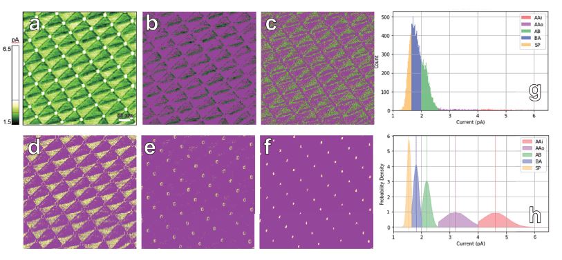
Figure 5. Domains classification within the obtained current map of a moiré pattern at positive potential (+200 mV). (a) Current map showing the distribution of electric current signal. Each domain is labeled accordingly in separate maps (non-purple colored) as follows: (b) Saddle points (SP), (c) BA (Bernal stacking), (d) AB (Bernal stacking), (e) AA (Aligned stacking) _outer, and (f) AA_inner. (g) Distribution of conductivity represented by the value of electric current signal across the moiré pattern. (h) Corresponding probability density plot illustrating the probability density distribution of the electric current signal across the moiré pattern.
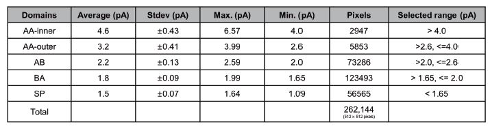
Table 1. Numerical domains classification within the obtained current map of a moiré pattern at positive potential (+200 mV).
Individual Domain Maps and Statistical Analysis of the Moiré Patterns under Negative Potential (Region B)
When subjected to negative potential, each domain was accurately identified using the current method (Figures 6), resulting in distinct domain maps without coupling (Figures 6b-f and Table 2). Although the AA domain was categorized into inner and outer regions (Figure 5e and 5f), the difference in current values was only 0.3 pA, significantly smaller than under positive potential but comparable to other domains within the same current map (Table 2). Additionally, the data distributions for each domain (Figure 6g) and the probability density (Figure 6h) further elucidate the vertical conductivity characteristics of this moiré pattern under negative electric potential. It is noted that the conductivity distribution is narrower compared to that under positive potential, ranging from – 0.95 pA to – 2.24 pA.
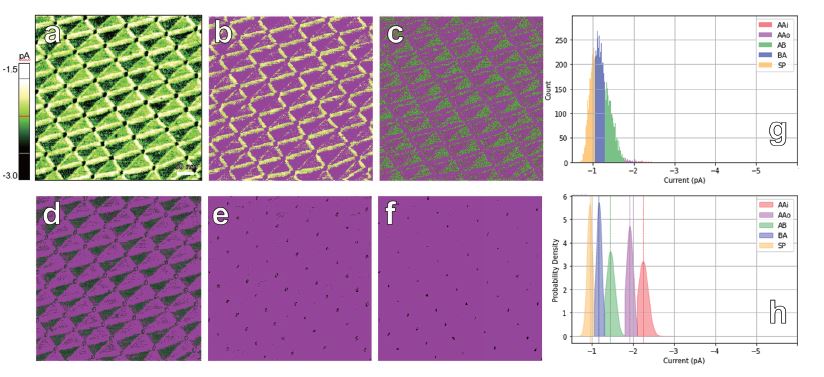
Figure 6. Domains classification within the obtained current map of a moiré pattern at negative potential (-200 mV). (a) Current map showing the distribution of electric current signal. Each domain is labeled accordingly in separate maps (non-purple colored) as follows: (b) Saddle points (SP), (c) BA (Bernal stacking), (d) AB (Bernal stacking), (e) AA (Aligned stacking) _outer, and (f) AA_inner. (g) Distribution of conductivity represented by the value of electric current signal across the moiré pattern. (h) Corresponding probability density plot illustrating the probability density distribution of the electric current signal across the moiré pattern.
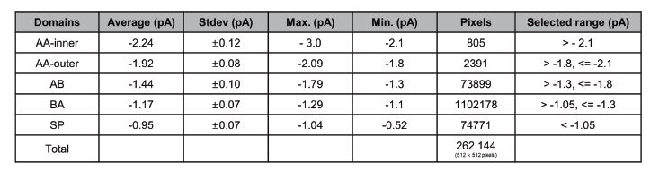
Table 2. Numerical domains classification within the obtained current map of a moiré pattern at negative potential (-200 mV).
Local Twisted Angle Calculation
Accurately determining the actual (local) twist angles in fabricated samples is crucial for the study of twisted 2D materials. The twist angle can be calculated using equation (1) provided below.14 In our measurements using C-AFM, the moiré patterns exhibited wavelengths (AA distance) of less than 80 nm. By knowing these specific AA distances, we calculated the corresponding twist angles. The calculated values for the series of moiré wavelengths are included in Table 3.
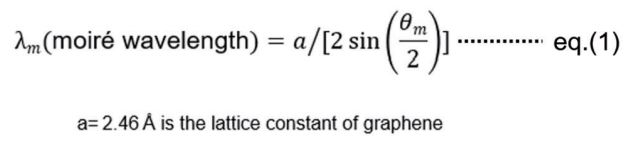
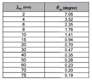
Table 3. Calculated local twisted angles as a function of moiré wavelength based on equation (1).
tBG Simulation and Corresponding Overlap Map (Twist Angle 2.35°)
To evaluate the correlation between the results obtained from C-AFM and the actual structure of graphene, tBG was constructed with repetitive honeycomb structures (the edge length of honeycomb: ca. 0.142 nm) (Figure 7). The construction was at the rotation angle of 2.35° which corresponds to the 6 nm moiré wavelength measured in region A. The simulation highlights areas of perfect alignment between honeycombs, referred to as AA regions (Figure 7a) including areas of misalignment, such as AB&BA and SP domains. To visually depict the AA region clearly, an overlap map was generated (Figure 7b). This map illustrates the intensity of overlap between the hexagonal basic unit cell of graphene layers, providing valuable insights into their alignment and orientation. The area of AA domain exhibits perfectly shaped honeycombs (red circles) while other areas with short lines for AB&BA (blue square) and dots for SP domains (grey rectangle). This overlap map facilitates the identification of AA domains, aiding in compara ive analyses. The current map of the moiré pattern measured in region A was compared with the corresponding overlap map (Figure 8). The 6 nm AA distance observed in the current map closely matched that of the simulation. Additionally, the positions of six AA domains in hexagonal shape aligned well with the simulation (dashed red circles in Figure 8a and b). This comparison underscores the accuracy of the moiré pattern obtained via C-AFM measurements, indicating minimal two-dimensional distortions.
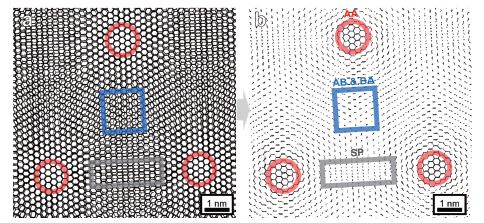
Figure 7. Twisted bilayer graphene simulation at a rotation angle of 2.35°. (a) Bilayer graphene with a hexagonal unit cell (the edge length of a single hexagon is 0.142 nm). (b) Overlap map of hexagonal unit cells created by logic OR operation binary image processing. In both images, AA domains are marked with red circles, AB & BA domains with blue squares, and SP domains with grey rectangles.
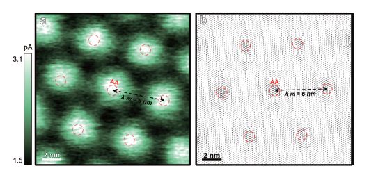
Figure 8. Comparison of experimental C-AFM measurement and simulated moiré patterns. (a) current map obtained from a moiré pattern of tBG in region A with an applied electric potential of +200 mV. AA domains are indicated by red circles, and the distance (moiré wavelength) between AA domains, λ, was estimated to be 6 nm. The local twisted angle was calculated as 2.35° using equation (1). (b) Overlap map of hexagonal unit cells, created at the same scale as (a) using logic OR operation binary image processing. The positions of the seven red circles in (b) are duplicated and placed in (a) for dimensional comparison, with a rotation applied for alignment of AA domains.
tBG Simulation and Corresponding Overlap Map (Twisted Angle 0.19°)
The moiré pattern measured in region B underwent the same comparison. In this pattern, AA distances were measured at three different lengths: 90 nm, 85 nm, and 52 nm, indicating an overall structure skewed in one direction. The average AA distance of 76 nm results in a twisted angle of 0.19°, significantly smaller than that observed in region A. As previously explained, each domain was clearly identified, facilitating the characterization of electrical properties from the recorded current map (Figure 9). The AA domain sizes were measured with an average diameter of 18.2 nm, an area of 179 nm², and a perimeter of 56.5 nm (Table 4).
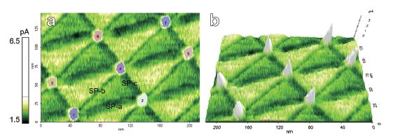
Figure 9. Current maps of the moiré pattern found in region B, measured by conductive AFM, with +200 mV, presented in 2D (a) and 3D (b).
The selected AA domains in (a) are depicted in different colors, each corresponding to a number for geometric analysis. In (a), three different
lengths of SPs within this moiré pattern were measured as 90 nm, 85 nm, and 52 nm, with an average length of 75.7 nm.
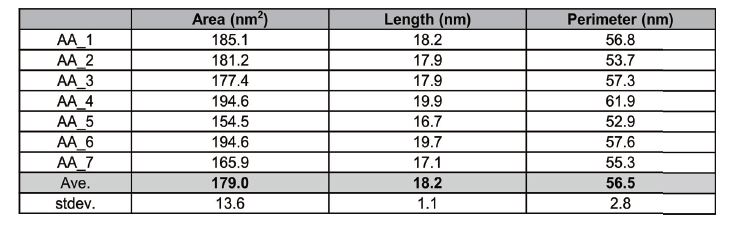
Table 4. Analysis of geometry for the selected AA domains depicted in Figure 9a, detailing area, volume, length, and perimeter.
The overlap map was also generated at various twisted angles less than that of region A, owing to the significantly longer moiré wavelength, which was approximately 12 times longer. Consequently, a significantly larger scale of the graphene 2D space was required for proper simulation, necessitating a massive number of hexagonal unit cells (Figure 10). An overlap map at a twisted angle of 0.19 degrees was generated in Figure 10a, exhibiting three zones with dark colors indicating AA domains. The two inset images show the overlap pattern of the AA domain (honeycomb) and SP domain (dots) (Figure 10a). The boundary of the AA domain was marked with a red dashed circle, and the AA distance (λm) was depicted with a black dashed arrow. As the twisted angle increases, the AA distance decreases, and the size of the AA domain also becomes smaller. This trend was measured and included in Table 5. The moiré wavelength at 0.19 degrees appeared to be 78.0 nm, and the size of the AA domain was measured as 17.6 nm. The result closely matched the values (76 nm and 18.2 nm) obtained from the current map, demonstrating the accuracy of C-AFM measurements of such moiré patterns of tBG at low rotation angles.
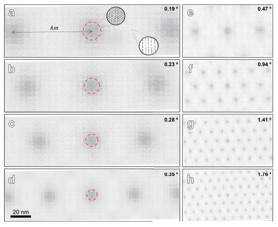
Figure 10. Simulated overlap map of hexagonal unit cells for twisted bilayer graphene at low rotation angles (a) 0.19°, (b) 0.23, (c) 0.28, (d) 0.35, (e) 0.47, (f) 0.94, (g)1.41, and (h) 1.76°. AA domains appeared to be in dark zone (represented as a red circle with a dashed line) in each simulated map. In (a), two inset images within grey circles exhibit the overlap pattern (zoomed-in) of hexagonal unit cells of each area. The moiré wavelength (λm), showing the distance between AA domains, is indicated by black dashed arrows.
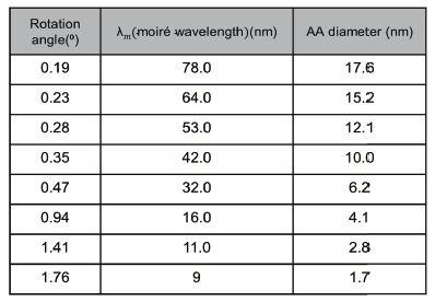
Table 5. Estimation of the moiré wavelength and the diameter of AA domains in low rotation angle measured from the simulation results presented in Figure 10.
Conclusions
We have demonstrated that Atomic Force Microscopy (AFM) offers exceptional sensitivity in current signal detection and precise length measurement. This enables accurate characterization of the electrical properties within each domain of the moiré pattern formed in low-angle twisted bilayer graphene (tBG). By accurately identifying local twist angles and mapping conductivity within the moiré pattern domains, AFM provides deep insights into the electronic properties of tBG. Additionally, anodic oxidation using a conductive AFM tip with AC voltage application is highly effective for cleaving graphene sheets into aligned segments, facilitating the fabrication of samples with the intended twist angle.
Low-angle tBG systems exhibit highly tunable electronic band structures, allowing for precise control of their properties through external parameters such as electric and magnetic fields. These characteristics make low-angle tBG an exciting platform for studying exotic quantum phenomena and developing next-generation electronic devices with enhanced functionality and performance. In this context, AFM analysis provides a powerful tool for advancing low-angle tBG research.
Finally, our research highlights the significant potential of this methodology utilizing C-AFM to advance the exploration of complex electrical phenomena in twisted bilayer systems of 2D materials.