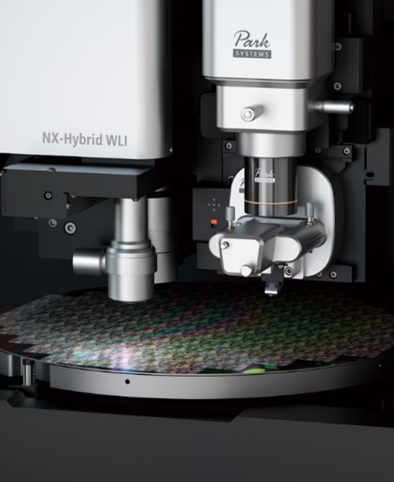
The AFM and White Light Interferometry(WLI) Technologies Built into One Seamless System
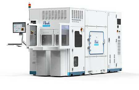
Park NX-Hybrid WLI is the first-ever AFM with built-in WLI profilometry for semiconductor and related manufacturing quality assurance, process control for semiconductor front-end, back-end up to advanced packaging, and R&D metrology. It is for those that require high throughput measurements over a large area that can zoom down to nanometer-scale regions with sub-nano resolution and ultra-high accuracy.
-
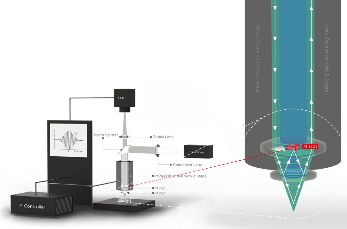
The Principles of WLI
A white light such as an LED or a halogen lamp is used as the light source to beam onto the sample through various lenses. While the sample is scanned with this beam, light intensity variations occur due to the light interference during the scan. Using this principle, WLI calculates the surface height at each point, producing a surface topography map.
-
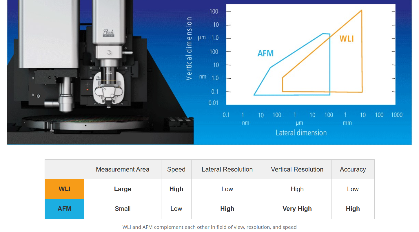
The Two Best Complementary Technologies
White light interferometry (WLI) and atomic force microscopy (AFM) are the two best complementary technologies for semiconductor metrology, with WLI offering fast, wide-area optical imaging for high throughput measurements, and AFM providing the highest nanoscale resolution, even for transparent materials.
-
Motorized Filter Changer
Park NX-Hybrid WLI supports both WLI and PSI modes, featuring a Motorized Filter Changer for PSI mode and an automated Motorized Linear Lens Changer that swiftly swaps between two objective lenses. Available magnifications include 2.5X, 10X, 20X, 50X, and 100X, enabling automatic replacement of lenses to suit diverse measurement needs.
-
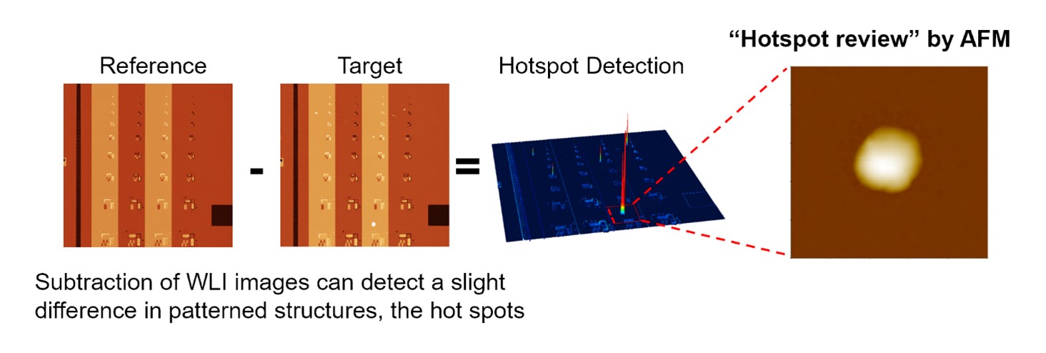
Application: Hotspot Detection and Review
Park NX-Hybrid WLI rapidly surveys hotspots and automates the review of hotspot defects by comparing images between reference and target sample areas, enabling high-speed 'hotspot detection.' This facilitates quick localization of defect sites for detailed, high-resolution AFM review.