FX40 with monitor

Park NX-Wafer

Industry’s Leading Automated AFM for In-line Metrology Solutions

Park NX-Wafer is the leading automated AFM system in the semiconductor industry. It offers comprehensive wafer fab inspection, defect review, and CMP profiling. Park NX-Wafer boasts the highest nanoscale surface resolution, consistent sub-angstrom height accuracy, and superior tip sharpness with minimal variation. Its features like auto tip exchange, live monitoring, markless target positioning, and automated analysis, make it a top-tier tool for semiconductor wafer applications.

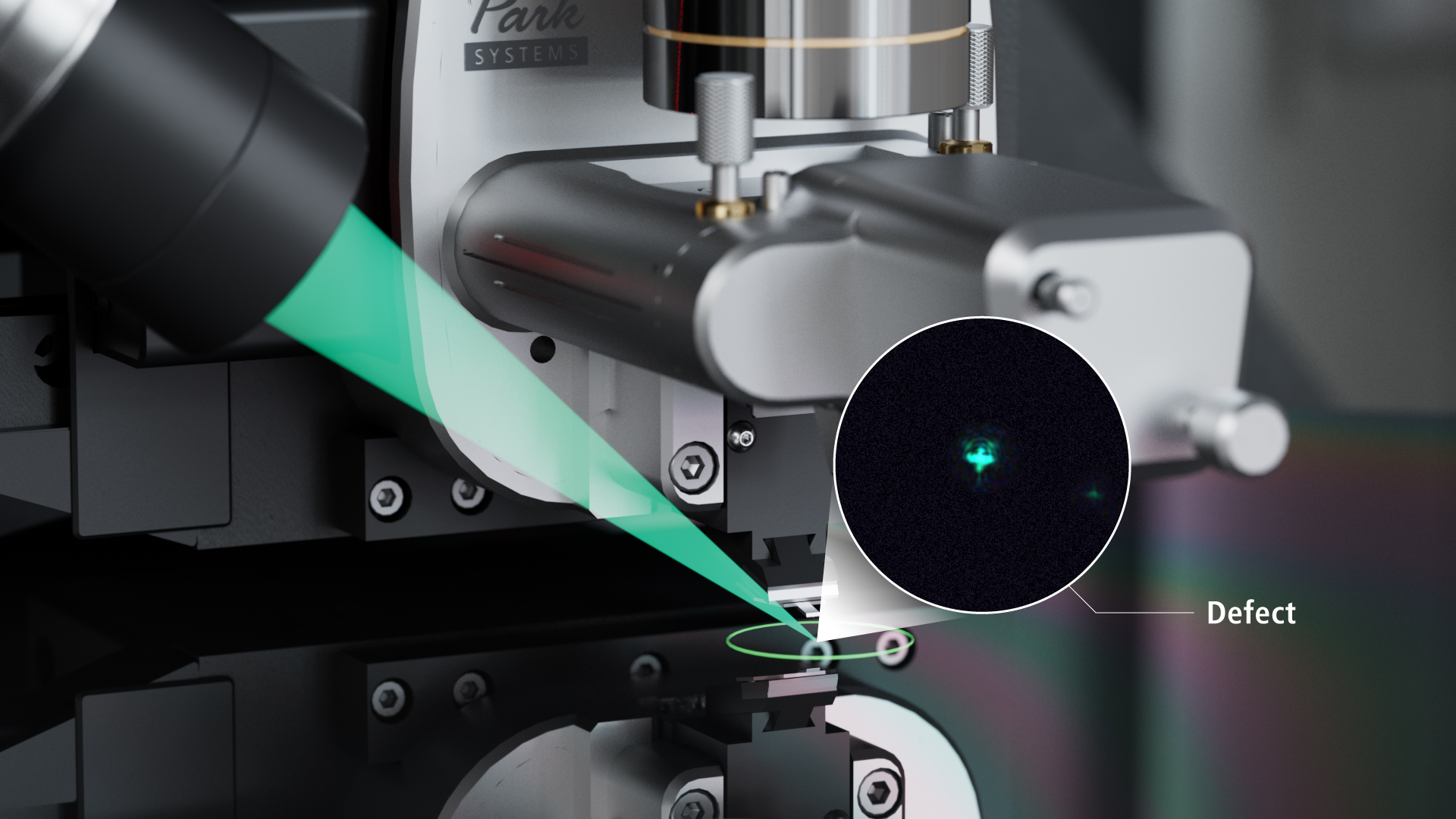
The Only Wafer Fab AFM with Automatic Defect Review

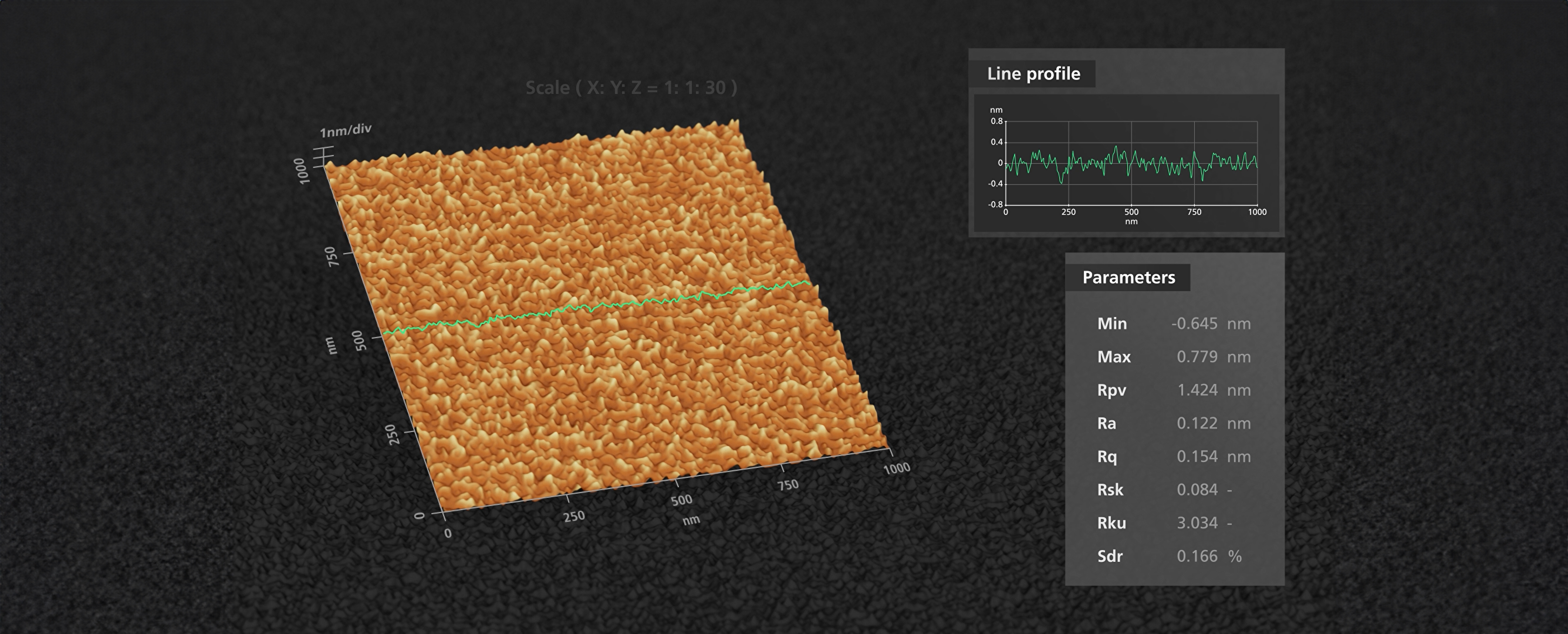
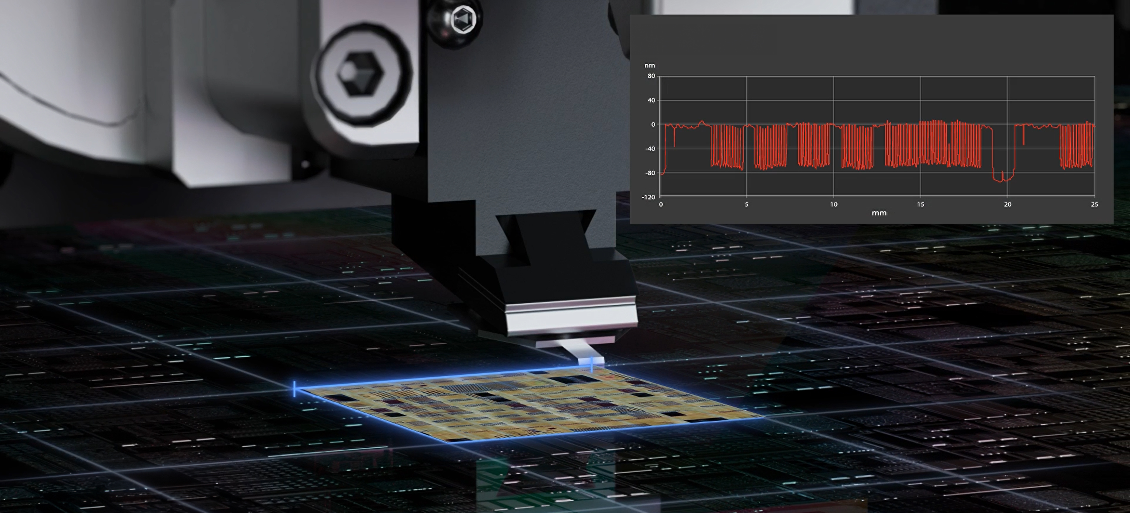
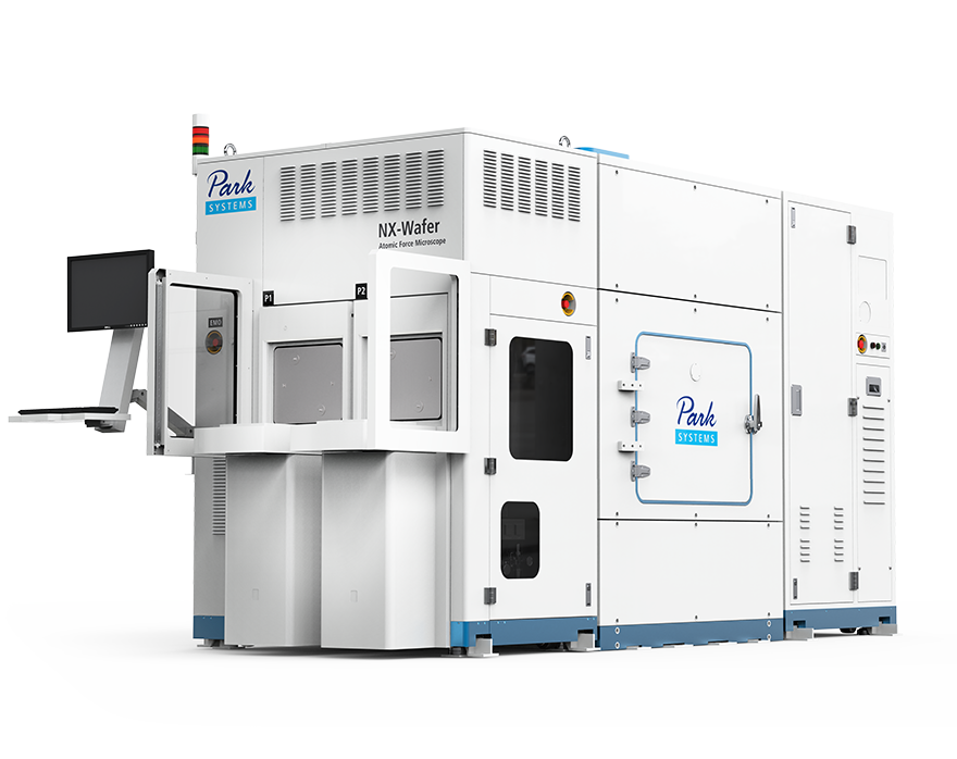
Park Systems Automated AFMs are engineered to excel wafer fabrication metrology, offering a precise toolset for critical measurements and analysis tasks. These advanced systems facilitate the detailed metrology required in semiconductor wafer fabrication, providing consistent, accurate, and extensive data that supports improved manufacturing processes and product quality. Designed to integrate seamlessly with existing fabrication lines, they deliver a robust solution for semiconductor production engineering and quality assurance. Park NX-Wafer is the industry’s leading automated AFM metrology system for semiconductor and related fabrications. It provides wafer fab inspection and analysis, automatic defect review for bare wafers and substrates, and CMP profile measurements. Park NX-Wafer has the highest nanoscale surface resolution with sub-angstrom height accuracy, scan after scan with negligible tip to tip variation and preserved tip sharpness unmatched by others. Park NX-Wafer with its automated system features including auto tip exchanger, live monitoring, target positioning without reference marks and auto analysis makes the best semiconductor AFM tool in the industry.

Revolutionizing Wafer Metrology with Advanced AFM

  • Automatic Defect Review for Bare Wafers

    The new 300 mm bare wafer ADR provides a fully automated defect review process from transfer and alignment of defect maps to the survey and zoom-in scan imaging of defects that uses a unique remapping process that does not require any reference marker on a sample wafer. Unlike SEM which leaves square-shaped destructive irradiation marks on defect sites after its run, the new Park ADR AFM enables advanced coordinate translation with enhanced vision that uses the wafer edge and notch to automatically enable linkage between a defect inspection tool and the AFM. Since it is fully automated, it does not require any separate steps to calibrate the stage of the targeted defect inspection system, increasing throughput by up to 1,000%.

    Automatic Defect Review for Bare Wafers
  • Sub-Angstrom Surface Roughness Control

    Semiconductor suppliers are developing ultra-flat wafers to address the ever-increasing need for shrinking device dimensions. However, there has never been a metrology tool capable of providing accurate and reliable measurements for the sub-Angstrom roughness of these substrate surfaces. By delivering the industry’s lowest noise floor of less than 1 Å throughout the wafer area, and combining it with True Non-Contact™ mode, the Park NX-Wafer can make accurate, repeatable, and reproducible sub-Angstrom roughness measurements for the flattest substrates and wafers with minimized tip-to-tip variation. Very accurate and repeatable surface measurements can be obtained even for the long-range waviness measurement of scan sizes up to 100 μm x 100 μm.

    Sub-Angstrom Surface Roughness Control
  • Long Range Profiling for CMP Characterization

    Planarization is the most important step in the back-end processes where metals and dielectric materials are used. Both local and global uniformity after chemical mechanical polishing (CMP) affect the yield of chip manufacturing significantly. Accurate CMP profiling is a critical metrology necessary to optimize process conditions for best planarity and improve production yield. Combining Park NX-Wafer with a sliding stage provides a long range profiling capability for CMP metrology. Due to the unique stage design of Park's automated AFM, the combined system provides very flat profiling and there is no need for complex background subtraction or past processing after each measurement in general. The Park NX-Wafer enables unprecedented CMP metrology of both local and global planarity measurements including dishing, erosion, and edge-over-erosion (EOE).

    Long Range Profiling for CMP Characterization

Automatic Tip Exchange (ATX)​

The ATX automatically locates tips by pattern recognition and uses a novel magnetic approach to disengage a used tip and pick up a new tip, with an incredible 99.9% success rate. The laser spot is then automatically optimized along the X- and Y-axis by motorized positioning knobs.

Ionization System for a more stable scanning environment​

Our innovative ionization system quickly and effectively removes electrostatic charges in your sample's environment. Since the system always generates and maintains the ideal balance of positive and negative ions, it can create an extremely stable charge environment with little contamination of the surrounding area and minimal risk of accidental electrostatic charge during sample handling.​

Automatic Wafer Handler (EFEM or FOUP)

The NX-Wafer also can be configured for various automatic wafer handlers (EFEM, FOUP, or other). The high-precision, nondestructive wafer handler robot arm fully ensures users always get fast and reliable wafer measurements.

100 µm x 100 µm Flexure-Guided XY Scanner with Closed-loop Dual Servo System

The XY scanner consists of symmetrical 2-dimensional flexure and high-force piezoelectric stacks that provide highly orthogonal movement with minimal out-of-plane motion, as well as the high responsiveness essential for precise sample scanning at the nanometer scale. Two symmetric, low-noise position sensors are incorporated on each axis of the XY scanner to retain a high level of scan orthogonality for the largest scan ranges and sample sizes. The secondary sensor corrects and compensates for non-linear and non-planar positional errors caused by a single sensor alone.

15 µm High Speed Z Scanner with Low Noise Position Sensor

The NX-Wafer provides you with unprecedented accuracy in topography height measurement by utilizing its ultra-low noise Z detector instead of the commonly used Z voltage signal that is non-linear in nature. This industry leading low noise Z detector replaces the applied Z voltage as the topography signal. Driven by a high-force piezoelectric stack and guided by a flexure structure, the standard Z scanner has a high resonant frequency of more than 9 kHz (typically 10.5 kHz) and Z-servo speed of more than 48 mm/sec tip velocity enabling more accurate feedback. The maximum Z scan range can be extended from 15 μm to 30 μm with the optional long range Z scanner.

Automatic Measurement Control

The NX-Wafer is equipped with automated software that makes operation nearly effortless. Just select the desired measurement program to get precise multi-site analysis with optimized settings for cantilever tuning, scan rate, gain, and set point parameters.

Applications

Perfect for Diverse Applications