


Biaxial Anisotropic Micro Crystals Investigated by Imaging Ellipsometry
SAMPLE:
Organic semiconducting micro crystals show high potential for the applications in microelectronic devices and flexible electronics due to the long-range-ordered molecular packing and absence of grain boundaries. The most organic single crystals indicates a highly anisotropic optical behaviour.
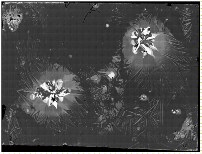
The semiconducting thiophene-phenylene cooligomer crystals were grown by solvent based self-assembly technique on silicon substrate with 300 nm thermally silicon dioxide. A ellipsometric high contrast map of the complete sample (right) indicates multi and mono layered crystals on the surfaces.
MEASUREMENT:
After rotating the sample into the pseudo-isotropic position we performed spectroscopic measurements (nanofilm_EP4, =400-700 nm) in 5 nm intervals at two different AOI.
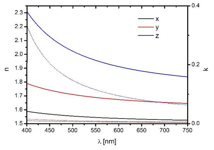
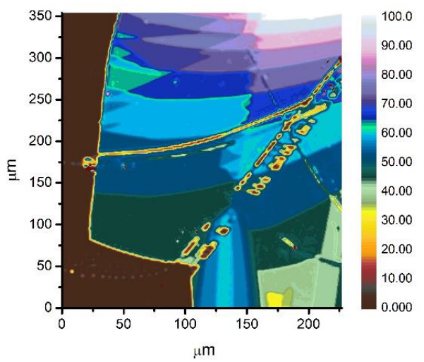
The optical properties were described by using a Lorentz term in the Ep4-Model. After determining the dispersion of the crystals (left) we converted a recorded Delta and Psi-map into a 2D thickness image (bottom right). Based on a quantitative analysis of the resulting thickness map we have calculated the height of a molecular layer.
RESULTS:
- Δ, Ψ values/maps for biaxial anisotropic micro crystals
- Fast observation and distinction between mono and multi layered micro crystal in high ellipsometric high contrast images
- Optical properties of biaxial semiconducting material
- Quantitative analyses of thickness map leads to the height of a molecular layer