


Characterization of Thin Films on Transparent Substrates with Imaging Ellipsometry
Introduction
Thin films on transparent substrates are of increasing interest in advanced technologies like flexible displays, plastic solar cells, functional windows or new concepts in illumination. State of the art in thin film metrology is spectroscopic ellipsometry, but transparent substrates are still an issue because of the backside reflected light that after a long pathway through a transparent substrate gets incoherent or partly coherent with the consequence that the phase information gets completely or partly lost and the determination of metrological parameters of the layer of interest is difficult or impossible. A number of workarounds are established to get rid of backside reflection, like mechanical grinder or a number of different treats of the backside with different types of tape, with glues, with toothpaste etc. A number of these approaches are working well but in most cases, the sample cannot be used for further investigations.
The main question is, how to suppress backside reflection in a nondestructive manner to optimize ellipsometric measurements on transparent substrates
Knife edge illumination
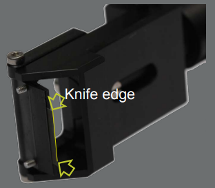
A very convenient and effective way to suppress backside reflected light is knife edge illumination to get a defined shadow behind the beam cutter
By moving the knife edge of the beam cutter into the beam of an imaging ellipsometer, the sample is illuminated with a well-defined edge.
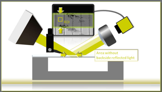
Also the backside reflected light still has a well defined edge and in relation to the internal angle of incidence it hits the surface in a distance to the knife edge. The shadow inbetween is free of contributions of backside reflected light.
For illustration purposes a backside roughened glass plate was used. The illuminated part of the backside as well as the shadow can be seen clearly. The same principle works also for much thinner substrates where the shadow is in the microscopic range. With an imaging ellipsometer, the measurements can also be performed in the microscopic shadow.
Ellipsometric enhanced contrast micrographs
In the ellipsometric enhanced contrast micrographs you can see clearly that the image quality in the shadow is much better than in the area with contributions of backside reflected light. In figure c, you see also disturbance from the backside like brighter strips and shadows of surface contaminations. All these effects disturb the measurement. It is obvious that the shadowed area is free of this disturbance.

a)
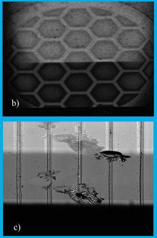
Ellipsometric enhanced contrast micrographs of Photoactive layer on PEDOT:PSS | ITO | PET (a) patterned coating on glass (b) and SiO2 (Nanoparticles) | glass (c)
Regions of Interest (ROI)
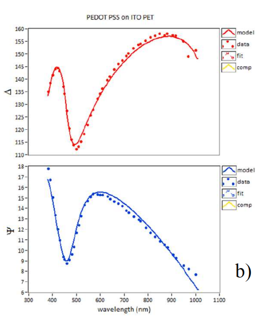
The detector of an imaging ellipsometer is a 2D CCD. Pixels, that display the region of interest on the sample can be selected to detect the ellipsometric angles only for this region of interest. In case of transparent substrates, the technique enable the measurement of delta and psi directly in the “shadow” of the beam cutter. The results like wavelength spectra of Delta and Psi can directly be used for the optical modeling.
Example:
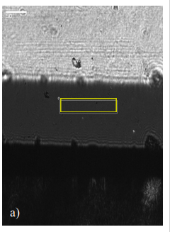
The image shows data of PEDOT:PSS on an ITO-PET substrate.
Image scan (a)
- 10x Objective - Lambda = 550 nm - AOI = 55° - FOV = 540 x 400 nm
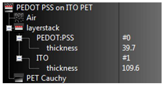
Two layers model, with PET as substrate, ITO layer, PEDOT:PSS layer on top and air as the ambient.
The PEDOT:PSS dispersion is modeled by a Tauc-Lorentz and a Drude term. The PET layer and the ITO layer were characterized in independent measurements.
Micro maps of Delta and Psi
A unique option of imaging ellipsometry is to use stacks of images at different orientations of the optical components to detect the delta and psi in pixel resolution. Depending on the objective the lateral resolution can be down to 1 nm.
Example:
MoS2-2D crystallites on a Sapphir substrate.
- The Delta and Psi maps:
10x Objective
Lambda = 400 nm
AOI = 50°
FOV = 510 x 435 nm
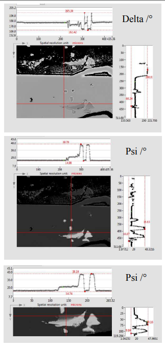
In the shadowed area, the values have a low noise level and the step between substrate and monolayerMoS2 monolayer is significant.
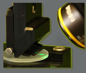
The new beam cutter for the nanofilm_ep4
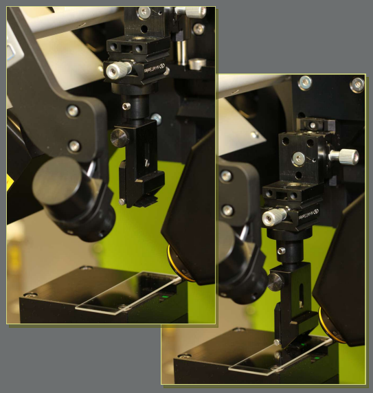
The open design of the nanofilm_ep4 enabled a new, very convenient setup: After an optimization it can be moved up and down easily. Changes in AOI and y,x-position can be done independently from the beam cutter.