FX40 with monitor

Park NX-Wafer

Industry’s Leading Automated AFM for In-line Metrology Solutions

Park NX-Wafer is the leading automated AFM system in the semiconductor industry. It offers comprehensive wafer fab inspection, defect review, and CMP profiling. Park NX-Wafer boasts the highest nanoscale surface resolution, consistent sub-angstrom height accuracy, and superior tip sharpness with minimal variation. Its features like auto tip exchange, live monitoring, markless target positioning, and automated analysis, make it a top-tier tool for semiconductor wafer applications.

The Only Wafer Fab AFM with Automatic Defect Review

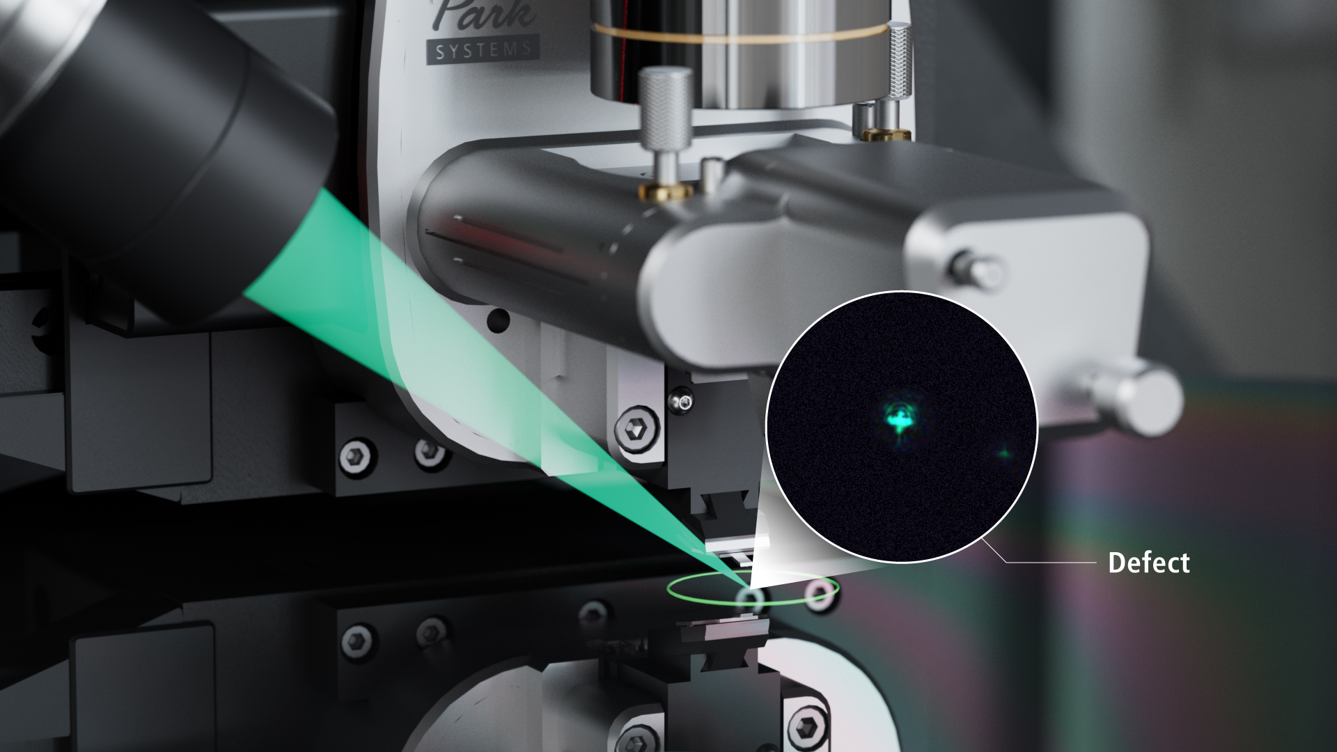
Park Systems의 Smart ADR은 결함의 검토 및 식별을 전자동으로 처리하며, 고해상도 3D 이미징을 통해 결점의 유형을 분류하며 결점의 근원을 찾는 중요한 인라인 공정을 가능하게 합니다. Smart ADR은 반도체 산업을 위해 특별히 설계된 가장 진보된 결함 검토 솔루션입니다. 이 결함 검토 솔루션은 샘플을 종종 손상시키며 많은 노동을 요구하는 참조 표시가 필요 없으며 자동 타깃 위치조절이 가능합니다. 기존의 결함 검토 방법들과 비교했을 때, Smart ADR 공정은 생산성을 최대 1,000%까지 개선시킬 수 있습니다. 또한, 새로운 ADR은 Park Systems만의 획기적인 완전 비접촉 모드TM 을 통해 팁의 수명을 최대 20배로 늘릴 수 있습니다.

Revolutionizing Wafer Metrology with Advanced AFM

  • Automatic Defect Review for Bare Wafers

    300mm의 새로운 웨이퍼 ADR은 결함 지도의 전송과 정렬부터 결함의 측량과 줌-인 스캔 이미징까지 전자동의 결함검토 공정을 제공하며, 이 공정은 샘플 웨이퍼에 참조 표시를 하지 않는 독특한 재배치 과정을 사용합니다. 사용 후 결함 장소에 사각형 모양의 파괴적인 조사 자국을 남기는 SEM과는 다르게, AFM에 의한 결함의 검토는 수 나노미터에 불과한 결함의 비파괴적인 3D 이미징이 가능합니다. 향상된 영상기법과 함께 진보된 좌표 변형은 결함 점검 툴과 AFM사이를 연결합니다. 웨이퍼 ADR은 전자동화가 되어있기 때문에, 목표 결함 검토 시스템을 보정하기 위한 단계를 설정하지 않으며, 스루풋을 최대 1,000% 가량 증가시킵니다.

    Automatic Defect Review for Bare Wafers
  • Sub-Angstrom Surface Roughness Control

    디바이스의 크기가 날로 줄어들고 있기 때문에 반도체 공급업체들은 극도로 평평한 웨이퍼를 개발하고 있습니다. 하지만, 아직까지 옹스트롬 이하의 거칠기를 가진 기판의 표면을 정확하게 측정하는 계측 툴은 존재하지 않았습니다. 시장 내 최저 수준인 0.5 Å미만의 노이즈 플로어를 제공하는 것과 더불어 Park Systems의 완전 비접촉 모드 TM를 탑재한 NX-Wafer는 최소한의 팁-팁 변화를 가지고 매우 평평한 기판과 웨이퍼의 옹스트롬 이하의 거칠기를 정확하고 반복할 수 있으며, 복제할 수 있게 측정합니다. 최대 100m x 100m 크기의 광범위한 파형의 스캔 측정도 매우 정확하고 반복적으로 할 수 있습니다.

    Sub-Angstrom Surface Roughness Control
  • Long Range Profiling for CMP Characterization

    금속재료와 유전체가 사용된 말기 공정에서 평탄과는 가장 중요한 단계입니다. 화학적 기계적 연마(CMP) 이후에 제품의 지역적 그리고 세계적인 균일성은 칩 생산량에 상당한 영향을 끼칩니다. 정확한 CMP 프로파일링은 최고의 평탄성과 제품의 높은 수율을 위해 매우 중요한 계측법 입니다. Park Systems의 NX-Wafer는 이동 스테이지와 함께 CMP 계측을 위한 광범위 프로파일링이 가능합니다. Park Systems의 자동 AFM만의 독특한 스캐너 설계에 의해, 시스템은 매우 평평한 프로파일링을 제공하며 각각의 측정 이후의 복잡한 배경제거 혹은 보정을 요구하지 않습니다. NX-Wafer는 디싱, 부식, EOE를 포함한 평면성 측정에 있어서 최고의 CMP 계측법을 제공합니다.

    Long Range Profiling for CMP Characterization

Automatic Tip Exchange (ATX)​

The ATX automatically locates tips by pattern recognition and uses a novel magnetic approach to disengage a used tip and pick up a new tip, with an incredible 99.9% success rate. The laser spot is then automatically optimized along the X- and Y-axis by motorized positioning knobs.

Ionization System for a more stable scanning environment​

Our innovative ionization system quickly and effectively removes electrostatic charges in your sample's environment. Since the system always generates and maintains the ideal balance of positive and negative ions, it can create an extremely stable charge environment with little contamination of the surrounding area and minimal risk of accidental electrostatic charge during sample handling.​

Automatic Wafer Handler (EFEM or FOUP)

The NX-Wafer also can be configured for various automatic wafer handlers (EFEM, FOUP, or other). The high-precision, nondestructive wafer handler robot arm fully ensures users always get fast and reliable wafer measurements.

100 µm x 100 µm Flexure-Guided XY Scanner with Closed-loop Dual Servo System

The XY scanner consists of symmetrical 2-dimensional flexure and high-force piezoelectric stacks that provide highly orthogonal movement with minimal out-of-plane motion, as well as the high responsiveness essential for precise sample scanning at the nanometer scale. Two symmetric, low-noise position sensors are incorporated on each axis of the XY scanner to retain a high level of scan orthogonality for the largest scan ranges and sample sizes. The secondary sensor corrects and compensates for non-linear and non-planar positional errors caused by a single sensor alone.

15 µm High Speed Z Scanner with Low Noise Position Sensor

The NX-Wafer provides you with unprecedented accuracy in topography height measurement by utilizing its ultra-low noise Z detector instead of the commonly used Z voltage signal that is non-linear in nature. This industry leading low noise Z detector replaces the applied Z voltage as the topography signal. Driven by a high-force piezoelectric stack and guided by a flexure structure, the standard Z scanner has a high resonant frequency of more than 9 kHz (typically 10.5 kHz) and Z-servo speed of more than 48 mm/sec tip velocity enabling more accurate feedback. The maximum Z scan range can be extended from 15 μm to 30 μm with the optional long range Z scanner.

Automatic Measurement Control

The NX-Wafer is equipped with automated software that makes operation nearly effortless. Just select the desired measurement program to get precise multi-site analysis with optimized settings for cantilever tuning, scan rate, gain, and set point parameters.

Applications

Perfect for Diverse Applications