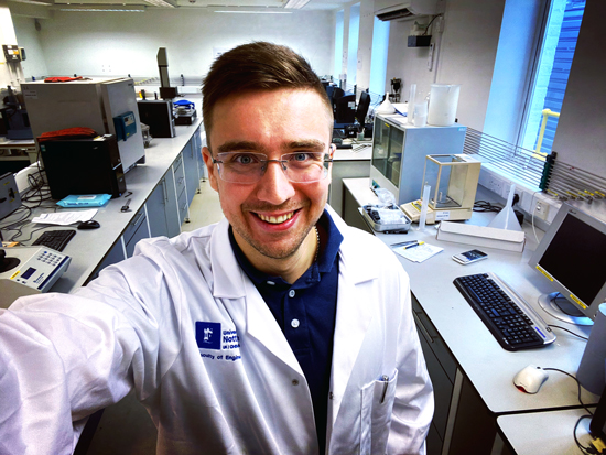
Dr Zakhar Kudrynskyi is a Research Fellow at the Faculty of Engineering, the University of Nottingham, UK. He studied at Chernivtsi National University in Ukraine where he graduated with first-class honours in Computer Engineering in 2010. Following that, he obtained his PhD in Physics of Semiconductors and Dielectrics at the Institute for Problems of Materials Science, National Academy of Sciences of Ukraine, Chernivtsi, Ukraine, in 2014. After his PhD, Dr Kudrynskyi worked abroad and in the School of Physics and Astronomy at the University of Nottingham, UK. In 2020 he joined the Advanced Materials Research group in the Faculty of Engineering at Nottingham. Currently, his main interests involve the science and technologies of innovative thin-film coating materials for electrical machines, power electronics, aerospace and renewable energy sectors.
1. Please summarize the research you do and explain why it is significant.
My current research is focused on the development of a novel class of high-performance, purely inorganic, electrically insulating materials designed using the concept of multi-layered thin films. These materials exploit the high thermal conductivity and dielectric strength of selected ceramic compounds, such as metal nitrides, to deliver a step change in the existing electrical and thermal limits in operational conditions: namely permitting continuous operation with high thermal conductivity at high temperatures ≥ 600°C and voltages ≥ 1.5 kV AC/DC, far beyond the capabilities of any existing electrical insulation.
2. How might your research be used?
This research aims to develop a radical innovation in electrification technologies previously infeasible with present electrically insulating coatings and manufacturing methods. My long-term ambition is to bring these coating materials from laboratories to everyday use, where they can really make a difference in a wide range of technologies, e.g., renewable energy, electric vehicles, hybrid aircraft (hydrogen/fully electric), industrial drives, robotics, low-carbon maritime and rail, offering innovative solutions to global challenges. This will be a vital step towards replacing fossil fuels with renewable powers to manage climate change and aligns with the UK government's ambitious target to reduce all greenhouse gas emissions to net-zero by 2050.
3. Why is the Park AFM important for your research?
The Park Systems NX20 large sample AFM equipped with high voltage tool kit and temperature controlled stage has been used in this research. This Park AFM enables different types of characterization of the surface of the ceramic thin films including: i) topographical characterization of the surface; ii) conductive atomic force microscopy measurements of leakage current and breakdown voltage at nanoscale; iii) determination of nanomechanical properties. The system offers a unique opportunity to combine all these measurements within a single piece of equipment and enables a significant acceleration of experimental measurements and high reproducibility of the obtained results.
4. What features of Park AFM are the most beneficial and why?
The NX20 is a state-of-the-art AFM combining unprecedented ease of use with a whole range of advanced imaging modes built into a single software package. The low-noise high-voltage amplifier and high temperature tool kit are key to this research project which studies high dielectric breakdown field strength of magnetron sputtered AlN thin films. In particular, the temperature-controlled stage enables to conduct measurements in a wide temperature range, namely from ambient temperature to 250 °C. The low-noise high-voltage amplifier for NX enables the application of high voltage bias up to ±150V (20x amplification ratio) to the samples. The unique capability to perform high voltage dielectric breakdown measurements whilst heating the sample up to 250°C makes it a perfect tool for investigation of thin-film samples for the most demanding applications.


