FX40 with monitor

Park NX-Wafer

自動欠陥レビュー機能を装備した低ノイズ、ハイスループット原子間力プロファイラー

Park NX-Waferは、半導体業界における最先端の自動AFMシステムです。ウェハーファブリケーションの包括的な検査、欠陥レビュー、CMPプロファイリングを提供します。Park NX-Waferは、最高水準のナノスケール表面分解能を持ち、一貫したサブオングストロームの高さ精度とばらつきを最小限に抑えた優れた探針の鋭さを誇ります。さらに、自動探針交換、ライブモニタリング、マークレスターゲット位置決め、自動解析などの高度な機能を備えており、半導体ウェハーアプリケーションにおける最高クラスのツールとなっています。

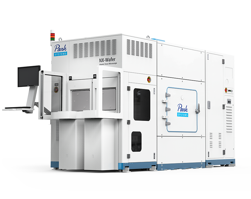
自動欠陥検査機能を搭載した唯一のウェハーファブ用AFM

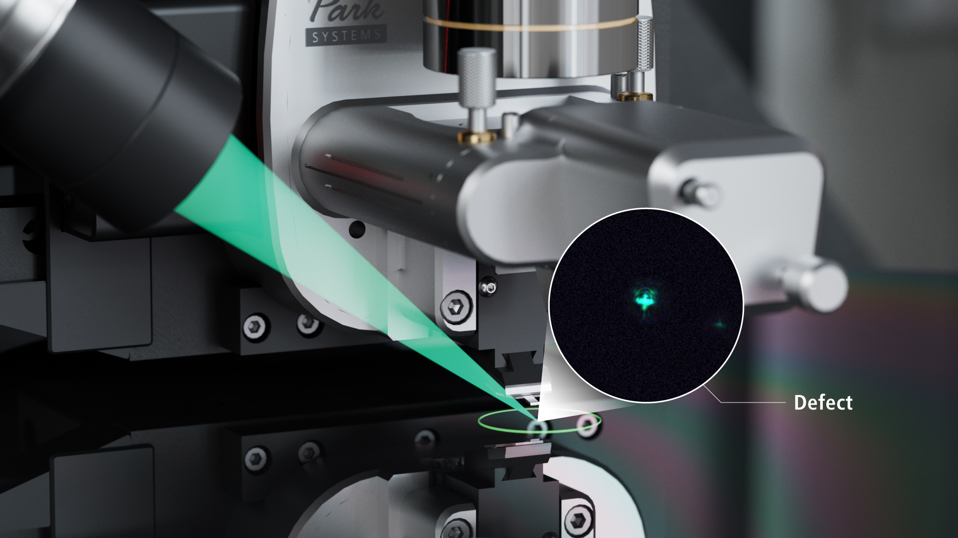
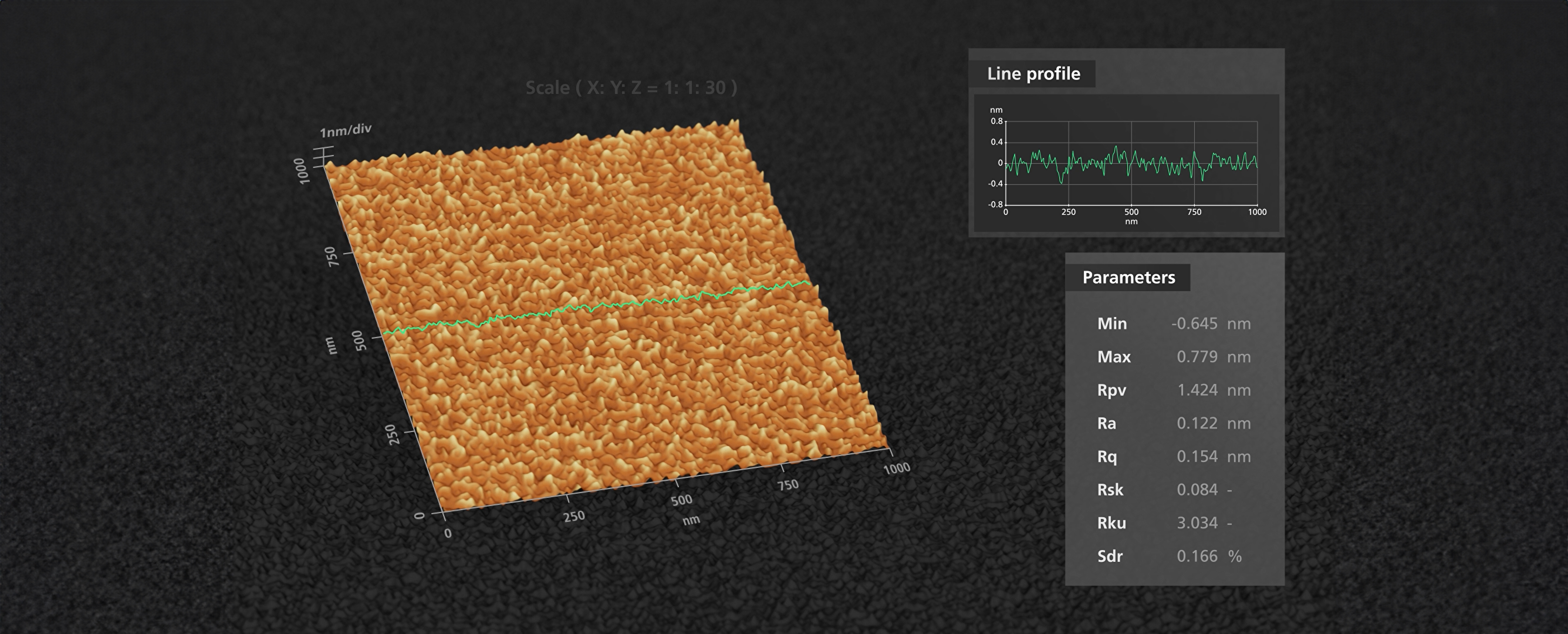
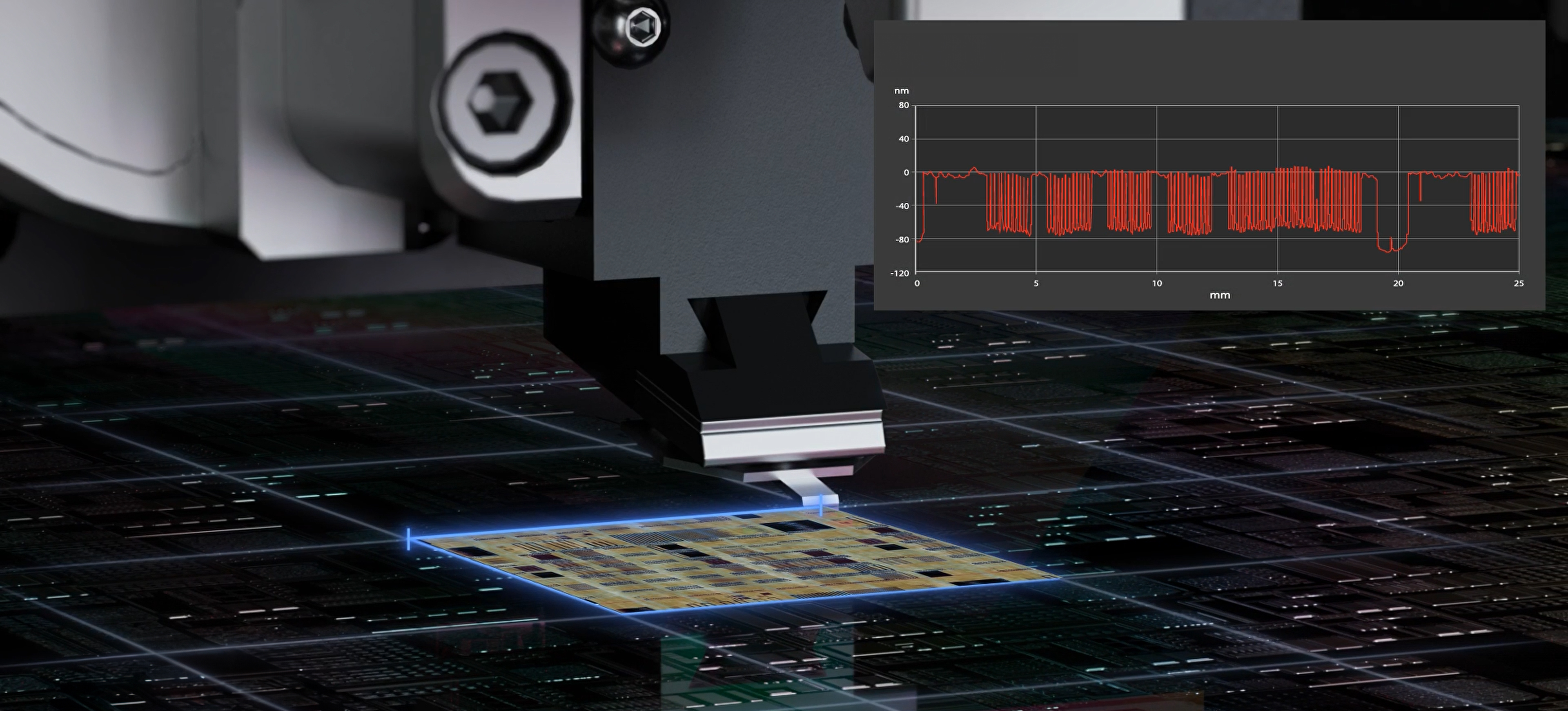
Park NX-Waferは、半導体および関連ファブリケーション向けの業界をリードする自動AFM測定システムです。ウェハーファブの検査と解析、ベアウェハーと基板の自動欠陥検査、およびCMPプロファイル測定を可能にするPark NX-Waferは、サブオングストロームの高さ精度を持つ最高のナノスケール表面分解能を持ち、チップ先端にダメージを与えずにスキャンを重ねることができます。 Park NX-Waferは、自動チップ交換、ライブモニタリング、リファレンスマークなしのターゲットポジショニング、自動解析などの自動化システム機能を備えており、業界最高水準の半導体AFM装置として位置付けられています。

インライン ウエハ計測の為の高い生産性と強力な機能

  • ベア ウエハとサブストレート用自動欠陥検査機能

    新しい300mmベア ウエハの自動欠陥検査(ADR)は、サンプル ウエハ上にマーキングすることなく欠陥のサーベイスキャンと拡大再スキャンを 行うユニークな機能を持ち、画像データの転送やアライメントも完全に自動で行うことができます。欠陥を観察した後に正方形の破壊的なビーム照射跡を残すSEMとは異なり、新しいPark ADRは、強化されたビジョン機能によりウエハのエッヂから座標を検出を行い外部の 欠陥検査ツールとAFMとの座標リンケージを自動的に行います。完全な自動化により、欠陥検査装置のステージを較正するステップを必要とせず、結果的に最大1,000%のスループットを向上させることができます。.

    ベア ウエハとサブストレート用自動欠陥検査機能
  • サブÅ表面粗さ制御

    半導体サプライヤーは、デバイス寸法が更に縮小化するニーズが増加する事へ対処するために、超フラット ウエハを開発しています。しかし、これらの基板表面のサブ オングストロームの粗さを正確で信頼性の高い測定が可能な計測ツールは、これまでありませんでした。ウエハ全領域で0.5A未満の業界最小のノイズフロアと真のノンコンタクト™モードを組み合わせることにより 、 Park NX-Waferは最もフラットな基板やウエハに対し、 チップ間のバラツキを最小化し、正確で再現性の高いサブ Å粗さ計測を実現しました。 最大走査サイズ100μm x 100μmの広範囲なうねり測定においても非常に 正確で再現性の高い表面測定ができます。

    サブÅ表面粗さ制御
  • CMP特性検査の為のロング レンジ プロファイリング機能

    平坦化は、メタルや誘電体材料が使用されているバックエンド プロセスの中で重要なテップです。化学機械研磨(CMP)後の局所的或いは広域における均一性は、チップ製造のスループットに非常に影響を及ぼします。正確なCMPプロファイリングは、平坦化のプロセスにおける生産性向上条件の最適化に必要とされる 非常に重要な計測技術です。 スライディングステージとPark NX-Waferを組み合わせることで、CMP計測における長距離プロファイリング機能が可能になりました。独自のスキャナ設計を持つPark社自動AFMは、 非常に平坦なプロファイリングを提供する為に、複雑なバックグラウンドの減算や、測定後の様々なキャリブレーションの必要がありません。Park NX-Waferはディッシング、エロージョン、エッジオーバーエロージョン(EOE)を含む居所的或いは、広域の平坦測定で前例のないCMP計測を可能にします。

    CMP特性検査の為のロング レンジ プロファイリング機能

Automatic Tip Exchange (ATX)​

The ATX automatically locates tips by pattern recognition and uses a novel magnetic approach to disengage a used tip and pick up a new tip, with an incredible 99.9% success rate. The laser spot is then automatically optimized along the X- and Y-axis by motorized positioning knobs.

Ionization System for a more stable scanning environment​

Our innovative ionization system quickly and effectively removes electrostatic charges in your sample's environment. Since the system always generates and maintains the ideal balance of positive and negative ions, it can create an extremely stable charge environment with little contamination of the surrounding area and minimal risk of accidental electrostatic charge during sample handling.​

Automatic Wafer Handler (EFEM or FOUP)

The NX-Wafer also can be configured for various automatic wafer handlers (EFEM, FOUP, or other). The high-precision, nondestructive wafer handler robot arm fully ensures users always get fast and reliable wafer measurements.

100 µm x 100 µm Flexure-Guided XY Scanner with Closed-loop Dual Servo System

The XY scanner consists of symmetrical 2-dimensional flexure and high-force piezoelectric stacks that provide highly orthogonal movement with minimal out-of-plane motion, as well as the high responsiveness essential for precise sample scanning at the nanometer scale. Two symmetric, low-noise position sensors are incorporated on each axis of the XY scanner to retain a high level of scan orthogonality for the largest scan ranges and sample sizes. The secondary sensor corrects and compensates for non-linear and non-planar positional errors caused by a single sensor alone.

15 µm High Speed Z Scanner with Low Noise Position Sensor

The NX-Wafer provides you with unprecedented accuracy in topography height measurement by utilizing its ultra-low noise Z detector instead of the commonly used Z voltage signal that is non-linear in nature. This industry leading low noise Z detector replaces the applied Z voltage as the topography signal. Driven by a high-force piezoelectric stack and guided by a flexure structure, the standard Z scanner has a high resonant frequency of more than 9 kHz (typically 10.5 kHz) and Z-servo speed of more than 48 mm/sec tip velocity enabling more accurate feedback. The maximum Z scan range can be extended from 15 μm to 30 μm with the optional long range Z scanner.

Automatic Measurement Control

The NX-Wafer is equipped with automated software that makes operation nearly effortless. Just select the desired measurement program to get precise multi-site analysis with optimized settings for cantilever tuning, scan rate, gain, and set point parameters.

Applications

Perfect for Diverse Applications