


Special Modes
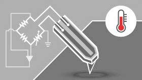
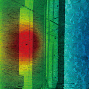
Scanning Thermal Microscopy (SThM)
High Spatial and Thermal Resolution Microscopy
Our SThM mode lets you easily find the local thermal conductivity of a sample by measuring heat transfer between tip and sample using a micro-fabricated probe.
Read More
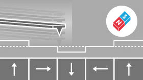
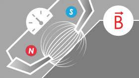
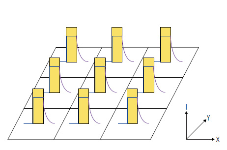
Magnetic Force Microscopy (MFM)
High Resolution and High Sensitivity Imaging of Magnetic Properties
Our MFM mode measures the magnetic variations over a sample surface by detecting the interaction between a magnetized cantilever and sample surface. The cantilever measures surface topography on the first scan, then lifts and follows either the stored surface topography (lift mode, available only in selected countries) or a constant distance (or constant height) at a fixed height above the sample surface.
Read More
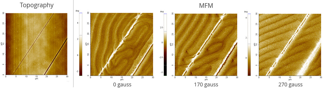
Tunable Magnetic Field MFM (TM-MFM)
High Resolution and High Sensitivity Imaging of Magnetic Properties
Our TM-MFM mode measures the magnetic domain distribution with respect to magnetic field change.
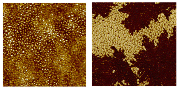
Chemical Force Microscopy (CFM)
CFM measures the chemical interactions between functionalized tips and sample to determine the chemical nature of surfaces and facilitate studies of chemical bonding enthalpy and surface energy. Tips are typically gold-coated and functionalized with R-SH thiols, R being the functional groups of interest such as -CH, -COOH, -NH, and -OH.
Electrochemical Microscopy (EC-AFM)
In EC-AFM, STM the nanoscale structures of electrochemical reactions on the electrode surface can be observed. Users typically perform voltammetry and corrosion experiments using an electrochemistry cell and a choice of potentiostat/galvanostat depending on the electrochemical application of interest.
Scanning Ion Conductance Microscopy (SICM)
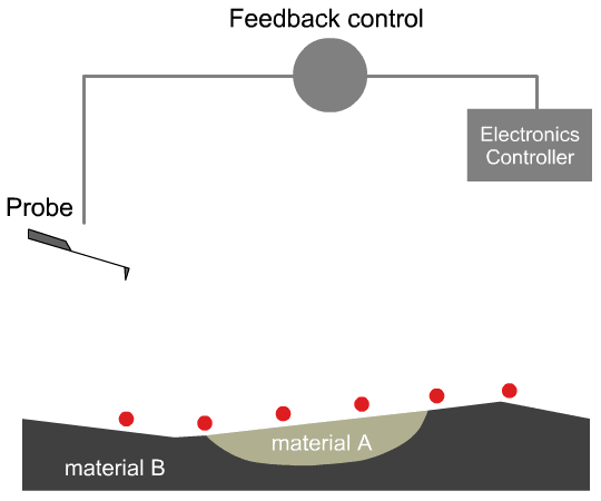
In Scanning Ion Conductance Microscopy developed by Park Systems (Park SICM), a glass nanopipette (a pipette in the nanoscale) filled with an electrolyte, acts as an ion sensor that provides feedback on its location relative to a sample completely immersed in a liquid. The pipette-tip maintains its distance from the sample by keeping the ionic current constant. In comparison, Atomic Force Microscopy (AFM) typically relies on interaction of forces between a probe tip and the sample.
Scanning ElectroChemical Cell Microscopy (SECCM)
Scanning probe microscopy (SPM), and especially pipette-based SPM techniques can offer new insights into the nano-scale chemical properties of the sample. Among the pipette-based SPM techniques, Scanning electrochemical cell microscopy (SECCM) is a recently developed pipette-based SPM technique designed to investigate the local electrochemical properties of surfaces. Using laser-pulled pipettes with nano or microscale tip radius, SECCM allows investigating electrochemical responses on target materials by applying a bias sweep, also known as cyclic voltammetry (CV).
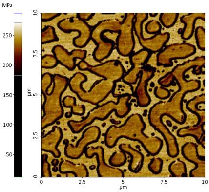
Nanomechanical Mode
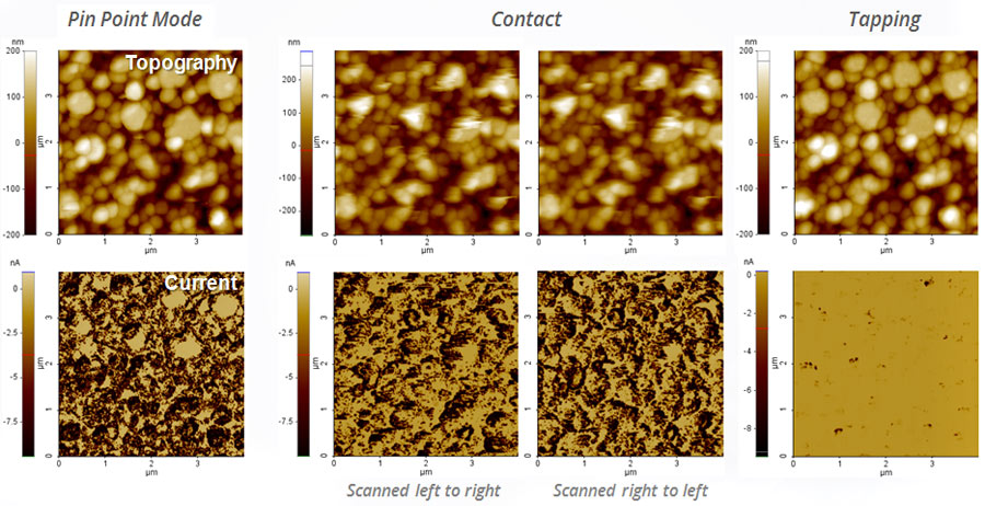
PinPoint™ Nanomechanical Mode

PinPoint™ Nanomechanical mode obtains the best of resolution and accuracy for nanomechanical characterization. Stiffness, elastic modulus, adhesion forces are acquired simultaneously in real-time. While the XY scanner stops, the high speed force-distance curves are taken with well-defined control of contact force and contact time between the tip and the sample. Due to controllable data acquisition time, PinPoint™ Nanomechanical mode allows optimized nanomechanical measurement with high signal-to-noise ratio over various sample surfaces.
Read MoreRead more about accurate Nanomechanical Imaging via PinPoint here
Video: Characterizing Multicomponent Polymer with PinPoint™ AFM
Force-Distance Spectroscopy
Force Measurement of Tip-Sample Interaction

Here, Force distance (FD) spectroscopy is a straightforward and reliable technique to quantitatively study nanomechanical properties such as Young’s modulus and adhesion force on a variety of samples. Therefore, FD spectroscopy has become a fundamental characterization tool in several fields of research, including polymer science, biochemistry, and biology.
Read More
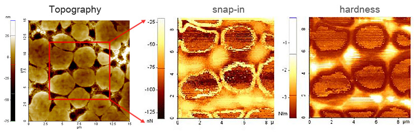
Force Volume Imaging
Force Measurement of Tip-Sample Interaction
Force volume imaging provides a detailed map of the sample’s material properties by plotting parameters such as stiffness, cantilever snap-in, and adhesion. Parameters extracted from Force Distance (F-D) spectroscopy curves are put into a matrix that quickly and easily allows researchers to gain insights about samples properties.
Force Modulation Microscopy (FMM)
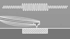
Force Amplitude and Phase Imaging of Sample Elasticity
In addition to topographic imaging, Atomic force microscopy (AFM) is routinely used to resolve mechanical properties of various samples for material and life science on the nanometer scale. An established technique to probe nanomechanical properties is Force modulation microscopy (FMM). FMM is based on contact mode AFM with an additional mechanical modulation that is applied to the cantilever during the contact scan.
Read More
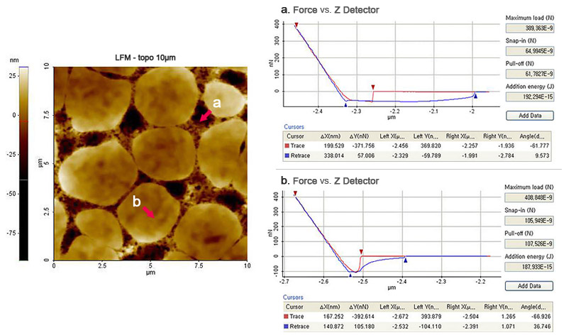
Lateral Force Microscopy (LFM)
Mapping of the Frictional Force
In AFM, frictional properties can be investigated via Lateral force microscopy (LFM). LFM can be used to study differences in material compositions on coating layers, lubricant properties, strength of adhesion on patterned structures and so on.
Read More
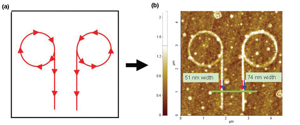
Nanolithography
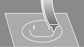
Advanced Vector Nanolithography Using Closed Loop Scan System
The Nanolithography mode allows you to manipulate and create patterning on the sample surface through applied force or voltage. Tip position for lithography can be easily controlled by importing your own vector drawings or raster (bitmap) images.
Read More
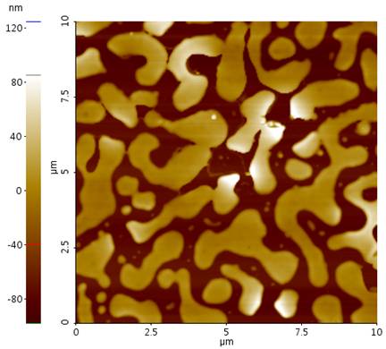
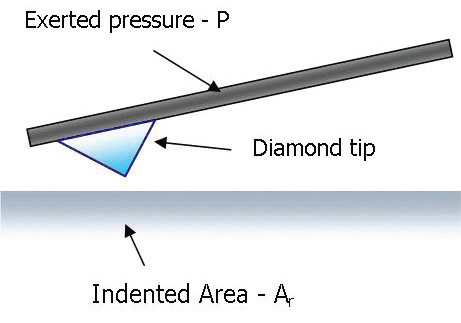
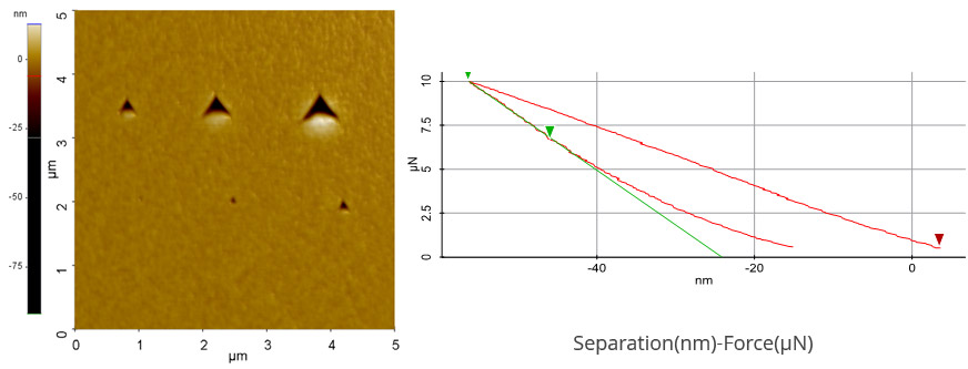
Nanoindentation
Atomic force microscopy (AFM)-based Nanoindentation quantitatively characterizes local mechanical properties of target specimen. In this technique, a hard AFM indentation tip with known mechanical properties presses against a sample surface until the tip deforms the surface.
Read More
Spring Constant Calibration by Thermal Method
Maintaining the proper spring calibration is critical for AFM force data accuracy. That’s why Park provides spring calibration using the thermal method, giving you accurate readings every time.
Imaging Modes
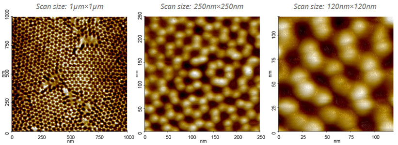
True Non-Contact™ Mode
Consistently produces high resolution and accurate data while maintaining the integrity of sample.
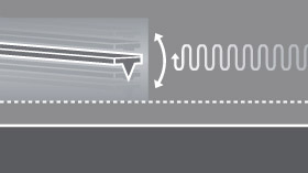
The True Non-Contact mode preserves tip sharpness and sample surface, and you can get more accurate results. In the True Non-Contact mode, a piezoelectric modulator vibrates a cantilever at small amplitude and a fixed frequency near the resonant frequency of the cantilever. As the tip is brought closer to the sample, the van der Waals attractive force between tip and sample changes the amplitude and the phase of the cantilever’s vibration. These changes are monitored by the patented Z-servo feedback system of the Park AFMs, which maintains a tip-surface distance of just a few nanometers without damaging the sample surface or the tip end.
Read More
Contact Mode

The simplest scanning method to image the surface
The contact mode is the simplest way to acquire the sample topography. The topography signal comes from the Z scanner position, which maintains the deflection of the cantilever constant on the sample surface.
Read More
Tapping Mode
In this alternative technique to non-contact mode, the cantilever again oscillates just above the surface, but at a much higher amplitude of oscillation. The bigger oscillation makes the deflection signal large enough for the control circuit, and hence an easier control for topography feedback. It produces modest AFM results but blunts the tip’s sharpness at a higher rate, ultimately speeding up the loss of its imaging resolution.
Read More
Electrical Modes
PinPoint™ AFM Nanoelectrical Modes
PinPointTM nanoelectrical modes eliminate lateral shear forces between the cantilever tip and the surface, thus minimizing damage while ensuring high imaging quality and reproducibility for a wide range of samples over many consecutive measurements. PinPoint can be combined with other AFM modes to obtain information about electrical properties such as:
• PinPoint Conductive AFM (C-AFM)
• PinPoint Piezoresponse Force Microscopy (PFM)
• PinPoint Scanning Spreading Resistance Microscopy (SSRM)
Brochures
PinPoint™ Conductive AFM obtains the best of resolution and sensitivity during current measurements
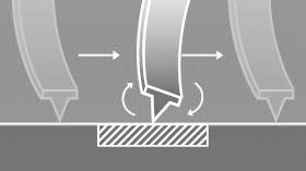
PinPoint™ Conductive AFM was developed for well defined electric contact between the tip and the sample. They XY scanner stops while measuring the electric current with contact time controlled by a user. PinPoint™ Conductive AFM allows higher spatial resolution, without lateral force, with optimized current measurement over different sample surface.
Learn more about how PinPoint mode enhances investigation of electrical and electromechanical properties here
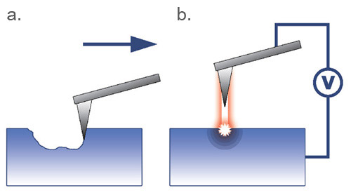
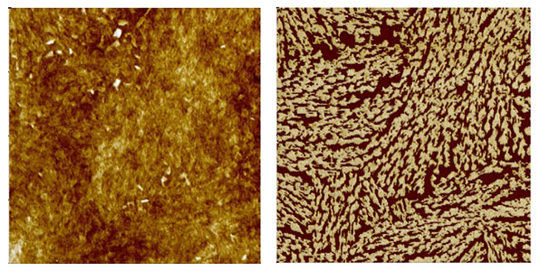
Conductive AFM (C-AFM)

Probing the Local Electronic Structure of a Sample’s Surface
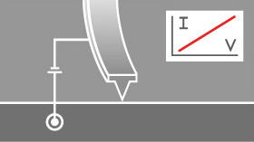
With the continuous decrease in device sizes and critical dimensions in the semiconductor industry, the ability to measure electrical properties locally with a high spatial resolution is vital for accurate device characterization and failure analysis. Here, Atomic force microscopy (AFM) offers real space imaging of local surface properties on the nanoscale. Conductive AFM (C-AFM) in particular, simultaneously measures the topography and conductivity of a sample by scanning the surface with a conductive material coated tip as a nanoscale electrical probe at an applied DC bias.
Read More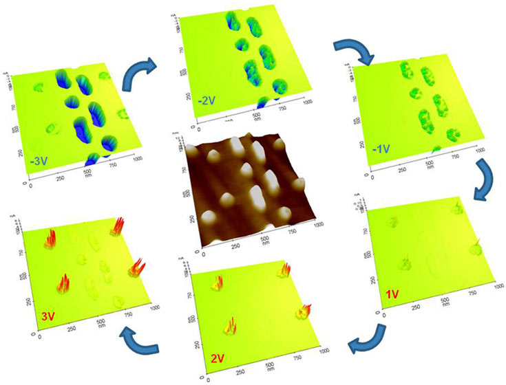
I-V Spectroscopy
Park AFMs feature the ability to conduct current voltage spectroscopy on specified point of the sample surface. The low noise of Park Systems’ conductive AFM options allows for the detection of extremely small changes in a sample’s electronic characteristics.
Read More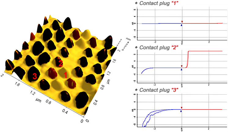
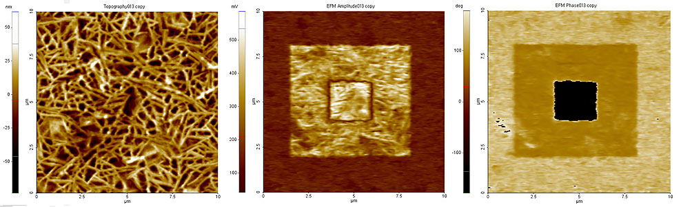
Electrostatic Force Microscopy (EFM)
High Resolution and High Sensitivity Imaging of Electrostatic Force
Almost every surface property measured by AFM is acquired by the process depicted. EFM measurements follow the same procedure. For EFM, the sample surface properties would be electrical properties and the interaction force will be the electrostatic force between the biased tip and sample. However, in addition to the electrostatic force, the van der Waals forces between the tip and the sample surface are always present. The magnitude of these van der Waals forces change according to the tip-sample distance, and are therefore used to measure the surface topography.
Read More
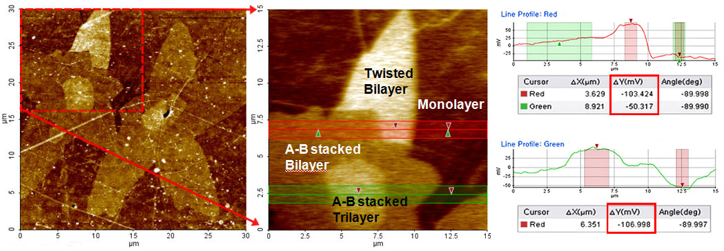
Kelvin Probe Force Microscopy (KPFM)
High Resolution and High Sensitivity Imaging of Surface Potential
Principle of KPFM is similar to Enhanced EFM with DC bias feedback. DC bias is controlled by feedback loop to zero the ω term. The DC bias that zeros the force is a measure of the surface potential. The difference is in the way the signal obtained from the Lock-in Amplifier is processed. As presented in previous section, the ω signal from Lock-in Amplifier can be expressed as following equation. scanning-kelvin-probe-microscopy-KPFM-f3 The ω signal can be used on its own to measure the surface potential. The amplitude of the ω signal is zero when VDC = Vs, or when the DC offset bias matches the surface potential of the sample. A feedback loop can be added to the system and vary the DC offset bias such that the output of the Lock-in Amplifier that measures the ω signal is zero. This value of the DC offset bias that zeroes the ω signal is then a measure of the surface potential. An image created from this variation in the DC offset bias is given as an image representing the absolute value of the surface potential.
Read More
Dynamic Contact EFM (DC-EFM)
High Resolution and High Sensitivity Imaging of Electrostatic Force
DC-EFM is capable of extremely high definition EFM results. Patented by Park Systems, DC-EFM actively applies an AC voltage bias to the cantilever and detects the amplitude and the phase change of the cantilever modulation with respect to the applied bias. DC-EFM provides the ability to monitor the second harmonic of the modulation which can be compared to the capacitance of a sample and enhances the electric force signal from the background intermolecular force.
Read More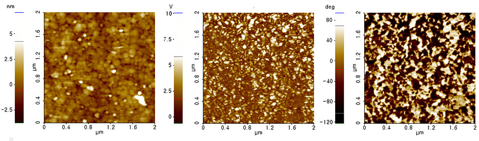
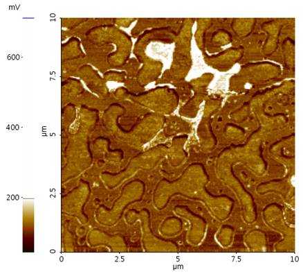
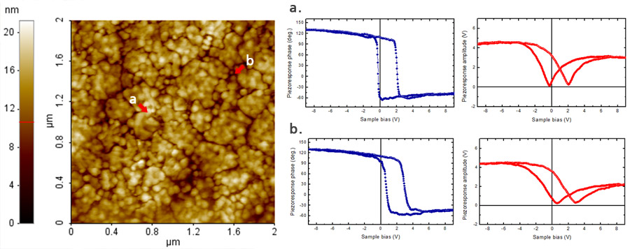
Piezoresponse Force Microscopy (PFM)
Piezoresponse force microscopy (PFM) is a functional Atomic force microscopy (AFM) mode, which probes electromechanical material properties on the nanometer scale in addition to the sample topography. As a conductive tip scans the surface in contact, an AC voltage introduces an electromechanical response in piezoelectric compounds and thereby resolves local variations of piezoelectric and ferroelectric properties. PFM has gained increasing recognition for the unique information it can offer on the electromechanical coupling characteristics of various materials including actuators, sensors, and capacitors for modern communication technology.
Read More
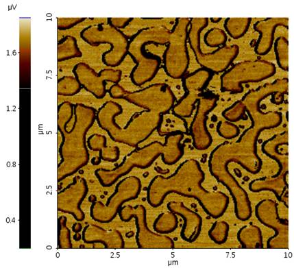
Piezoresponse Force Spectroscopy
Our Piezoresponse Force Spectroscopy mode measures the local amplitude/phase response to a DC bias between tip and sample surface. The polarity of local piezoelectric domain switches depend on the sign and amount of applied voltage.
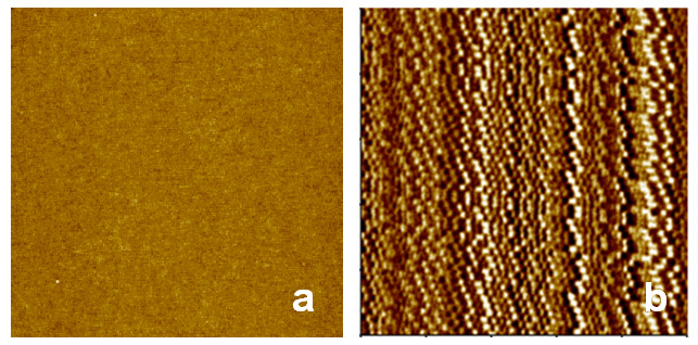
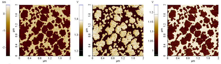
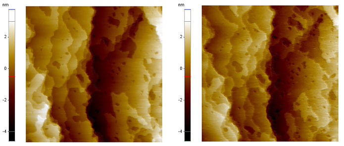
QuickStep™ SCM
 In QuickStep scan, the XY scanner stops at each pixel point to record the data. It makes a fast jump between the pixel points.
QuickStep™ to make faster SCM data acquisition
In order to improve the signal-to-noise ratio, conventional SCM adopts very slow scan speeds as a means of giving the detector enough time to collect the data. QuickStep™ SCM differs from the conventional methodology of slow continuous movement. Here, XY scanner stops at each pixel point to record the data and then makes a fast and rapid hop to the next measurement points. This effectively speeds up the scan rate while maintaining the same signal sensitivity of the measurements by conventional SCM at slow scan speeds.
Application note: Accurate dopant profiles of semiconductor device structures with QuickStep Scanning Capacitance Microscopy
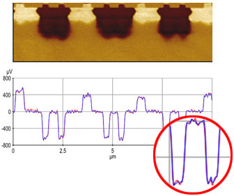 QuickStep Scan (Scan rate 1.5Hz)
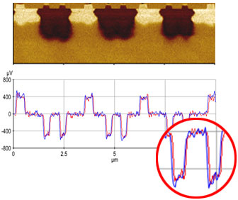 Conventional Scan (Scan rate 1Hz)
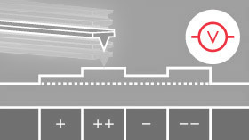
Scanning Capacitance Microscopy (SCM)

High Resolution and High Sensitivity Imaging of Charge Distribution
Our SCM mode provides doping concentration information over the sample surface by measuring the capacitance change between tip and sample. the module enables a variable resonator frequency, which allows a wide RF bandwidth capable of monitoring a large range of doping concentrations by selecting the most sensitive frequency of the resonator for a specific doping range.
Read More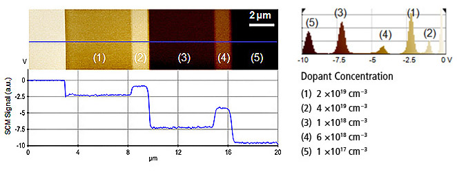
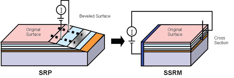
Scanning Spreading Resistance Microscopy (SSRM)

Probing the Local Electronic Structure of a Sample’s Surface
Our SSRM mode precisely measures the local resistance over a sample surface by using a conductive AFM tip to scan a small region while applying DC bias.
Read More
Scanning Tunneling Microscopy (STM)
Probing the Local Electronic Structure of a Sample’s Surface
STM measures the tunneling current between tip and sample, giving highly accurate sub-nanometer scale images you can use to gain insights into sample properties.
Read More
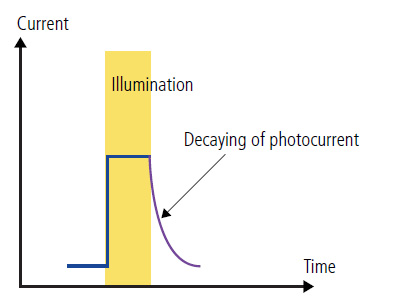
Photo Current Mapping (PCM)

Enabling Innovation in Photosensitive Materials Research
Our PCM mode measures photoelectric response to a illumination without interference from unwanted light sources, including the feedback laser. This mode features a laser illumination module and acquisition and analysis software.
Read More
Modes and Techniques
Get the data you need with Park's selection of scanning modes
Park AFMs feature a comprehensive range of scanning modes so you can collect a wide array of data types accurately and efficiently. From the world’s only true non-contact mode that preserves tip sharpness and sample integrity to advanced Magnetic Force Microscopy, Park offers the most innovative, accurate modes in the AFM industry.
Imaging Modes
Park offers some of the most innovative imaging modes and technology. Our True Non-Contact mode is the world’s only truly non-contact AFM scanning mode while our standard scanning mode is among the most accurate available.
Electrical Modes
For engineers and researchers that need accurate data on conductance, sample resistance, and other electrical and topographic properties, Park offers a range of electrical scanning modes.
Nanomechanical Modes
Easily measure the mechanical properties of your sample using our set of mechanical scanning modes. Each features Park System’s trademark accuracy so you always know
you’re collecting data you can rely on.