


Few Layers Graphene


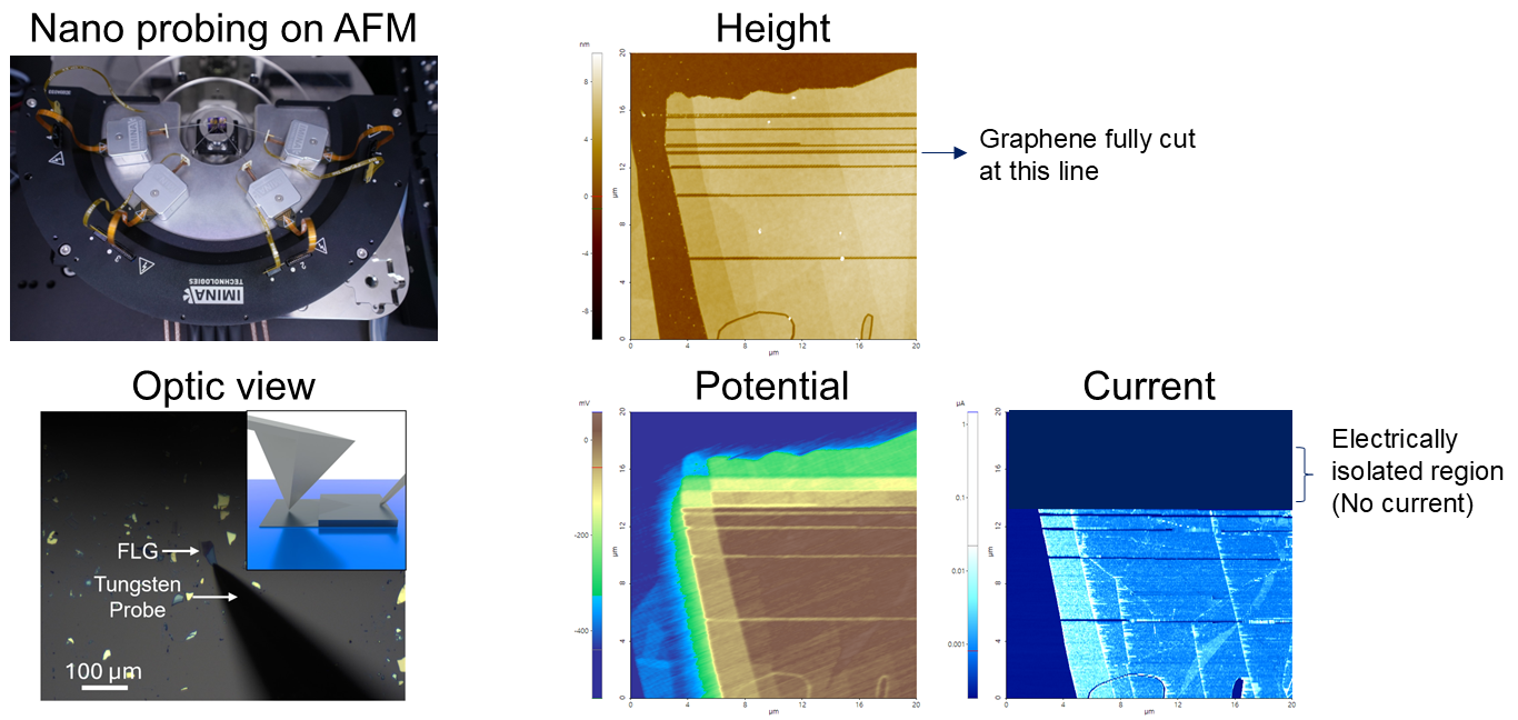
Electrically floating few-layer graphene (FLG) flakes were contacted by Nanoprobing Stage with a tungsten probe, and electrical lithography was performed several times to cut the flake in horizontal directions and create laterally isolated graphene regions.
Subsequent KPFM potential and Conductive AFM current imaging confirmed successful electrical isolation, showing no current in the cut region while the tungsten probe served as a ground reference.
Scan Conditions
- System: FX200
- Scan Mode: KPFM, C-AFM, Litho., Nanoprobing Stage
- Scan Size: 30 µm×20 µm
- Scan Rate: 0.2 Hz
- Pixels: 512×512
- Cantilever: Multi75E-G
(k=3 N/m, f=75 kHz)
Application
Related Products
Related Contents


×