


Adam Thomas Pierce
UC Berkeley physics graduate, MIM development at Park Systems
As semiconductor devices and advanced materials continue to shrink in scale and increase in complexity, the demand for precise nanoscale electrical characterization techniques is rapidly growing. Microwave Impedance Microscopy (MIM) has emerged as a powerful solution, offering researchers the ability to visualize local electrical properties with minimal sample preparation and high sensitivity.
From Research to Reality
Prof. Eric Ma's pioneering MIM research provides a foundation for the story behind Park's development effort. Adam Thomas Pierce brought experience from his work with Ma at UC Berkeley to his collaboration with Park Systems.
Together with Park's expertise in AFM instrumentation and system integration, that research background informs the development of a practical MIM solution. The ambition, reflected in Pierce's interview, is to make nanoscale electrical characterization accessible to more research laboratories.
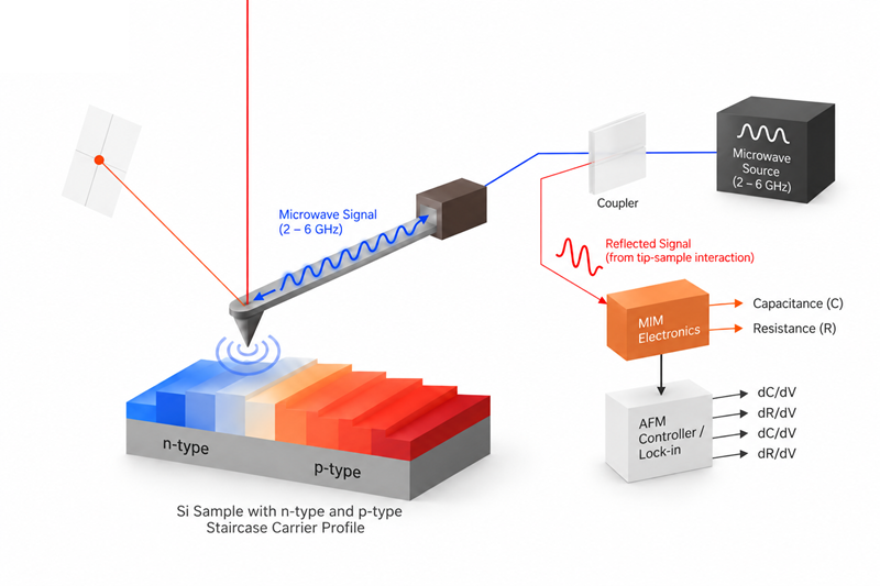
Figure 1. Microwave Impedance Microscopy system configuration for nanoscale electrical characterization of sample structures through non-destructive microwave signal detection.
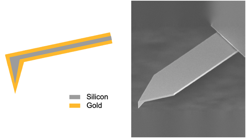
Figure 2. OPUS 160AC-GG, compatible with a range of conductive AFM probes.
What is Microwave Impedance Microscopy, and what can it reveal at the nanoscale?
Microwave impedance microscopy is an emerging scanning probe microscopy technique that allows us to take images of a sample's local electrical properties.
We perform this by sending microwave radiation through a conductive cantilever, and this microwave radiation is absorbed by the sample. Then, based on the tip-sample interaction, we can measure how that microwave radiation is reflected back at us and calculate the local capacitance and resistance of the sample. This gives us insight into lots of useful information about the system. We can calculate roughly the dielectric function of the sample, and this has lots of applications in semiconductor analysis, quantum materials, and lots of other avenues of research.
How are recent MIM system and probe developments improving performance at Park Systems?
Leveraging recent advances in literature, such as papers published by Dr. Eric Ma, we have designed a system that is capable of both contact and non-contact measurements using widely available conductive cantilevers. We have also developed a simplified microwave architecture, and this allows for more reliable and repeatable measurements at the same time as reducing noise. By using widely available conductive cantilevers, we allow for more flexibility in measurement techniques.
What advantages does MIM offer over conventional electrical characterization techniques?
There are a lot of techniques that are capable of measuring electrical properties of samples, such as conductive atomic force microscopy or scanning capacitance microscopy. All these techniques have their applications, but MIM has several advantages. One of the biggest advantages of microwave impedance microscopy is the very low requirement for sample preparation. Many other techniques require sample electrodes to apply a voltage bias to the sample; microwave impedance microscopy does not require this. And microwave impedance microscopy also does not need any specific surface preparation.
We can perform these measurements with an oxide layer or without an oxide layer, and we're a lot more flexible in the types of samples that we can easily measure. MIM is capable of measuring both conductive and dielectric samples, and this also gives us sensitivity to buried structures, such as if you have a buried metal via in a semiconducting sample, we have the capability to measure that which some other electrical techniques would not be able to do.
How can MIM measurements be stabilized against noise and drift?
Noise is inevitable in all measurements that you take, particularly for electrical measurements. But for MIM, there's some additional considerations that you need to take into account. You always have electromagnetic and acoustic interference from the environment that you need to work to shield against, and the different parts of your system can induce drift in your measurements or induce sources of noise that are avoidable. So by carefully choosing your system architecture, as well as very carefully constructing the environment that you're taking your measurements in, as well as careful choices of your probe and making sure that your probe-sample interaction is stable, you're able to minimize these effects.
What are the most promising applications for MIM moving forward?
Microwave impedance microscopy is really exciting, and there's a lot of interest and literature at the moment in exploring these techniques. There is a very large application in the semiconductor analysis area. Because of the high sensitivity and also low sample preparation needed for these measurement modes, you can perform high-throughput and reliable measurements of advanced semiconducting devices. There's also lots of very interesting research that I'm personally interested in, quantum materials. There's lots of literature that's using microwave impedance microscopy to explore interesting electronic states in two-D quantum materials. So, I think that MIM will play a big role in these fields going forward.
The flexibility of MIM really has some unique opportunities to explore multimodal measurement techniques. By combining microwave impedance microscopy with other AFM measurements as well as different external stimuli, such as optical stimuli, we can probe some really interesting properties of materials. And also, this technique is opening the door to more advanced measurements in chemical and biological systems. I hope that R&D advances that Park Systems is contributing to in microwave impedance microscopy can open the door to more research laboratories to take advantage of these unique advantages and push the field of MIM forward.


